Piezoelectric element, liquid ejecting head, and liquid ejecting apparatus
a liquid ejecting head and ejector technology, applied in the direction of device details, device material selection, device details, etc., can solve problems such as dielectric breakdown, and achieve the effects of suppressing the cracking of the piezoelectric layer, preventing dielectric breakdown, and reducing the voltag
- Summary
- Abstract
- Description
- Claims
- Application Information
AI Technical Summary
Benefits of technology
Problems solved by technology
Method used
Image
Examples
embodiment 1
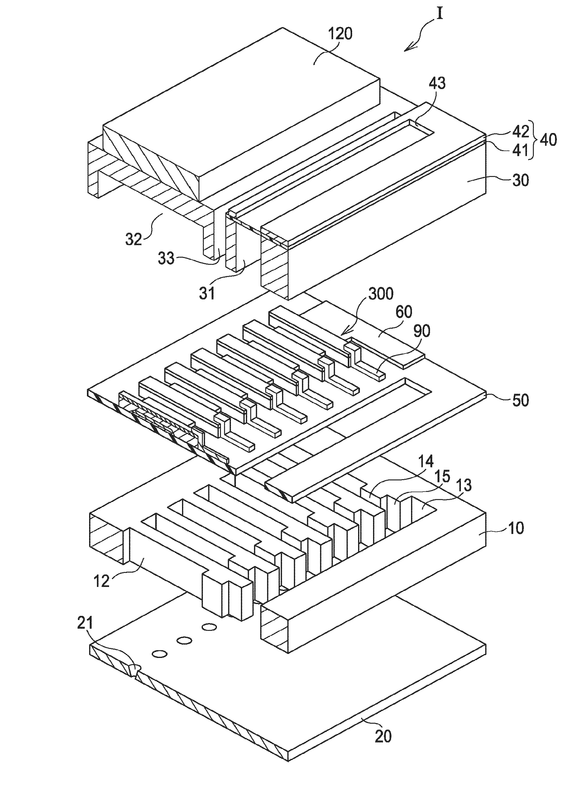
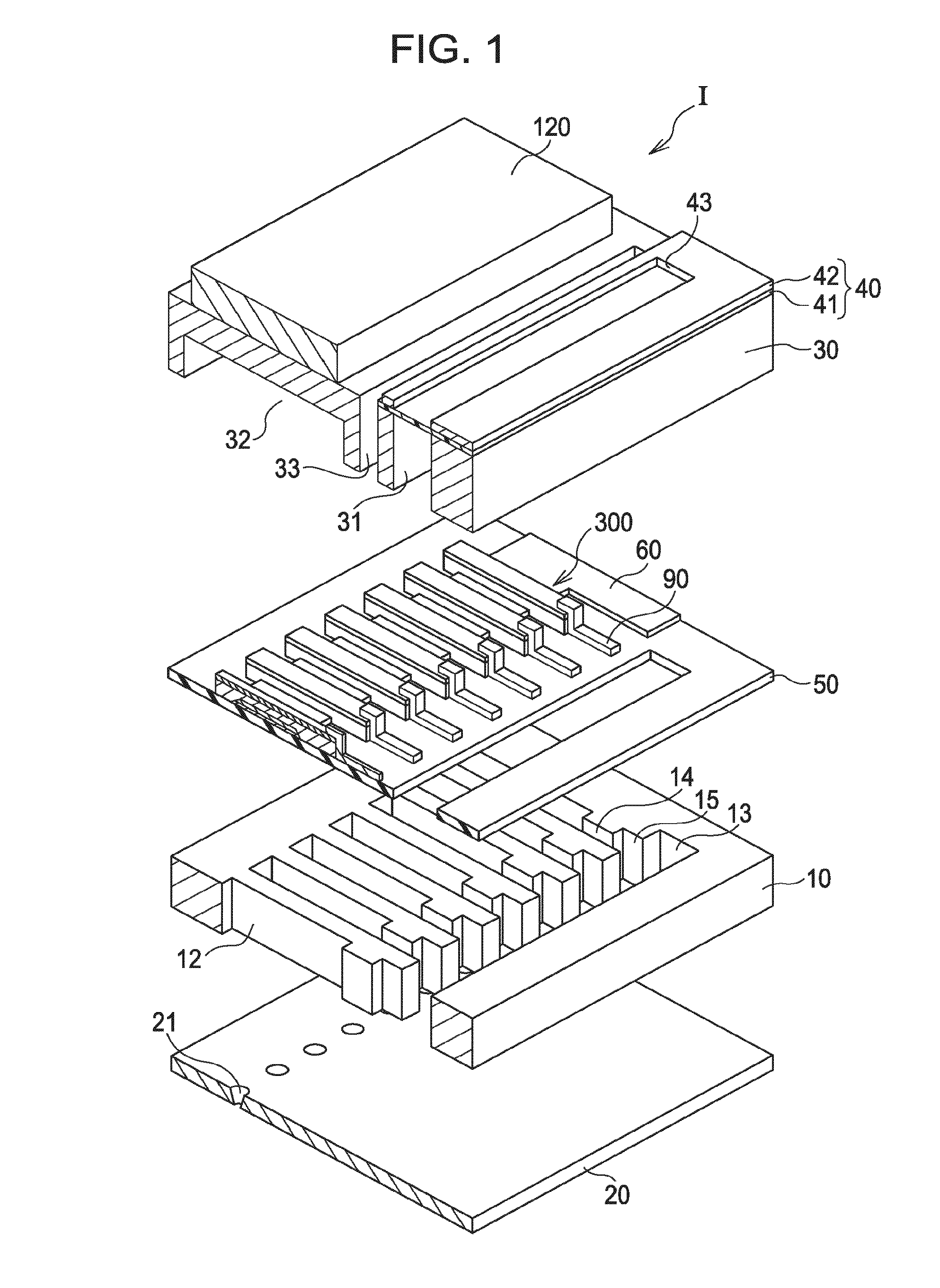
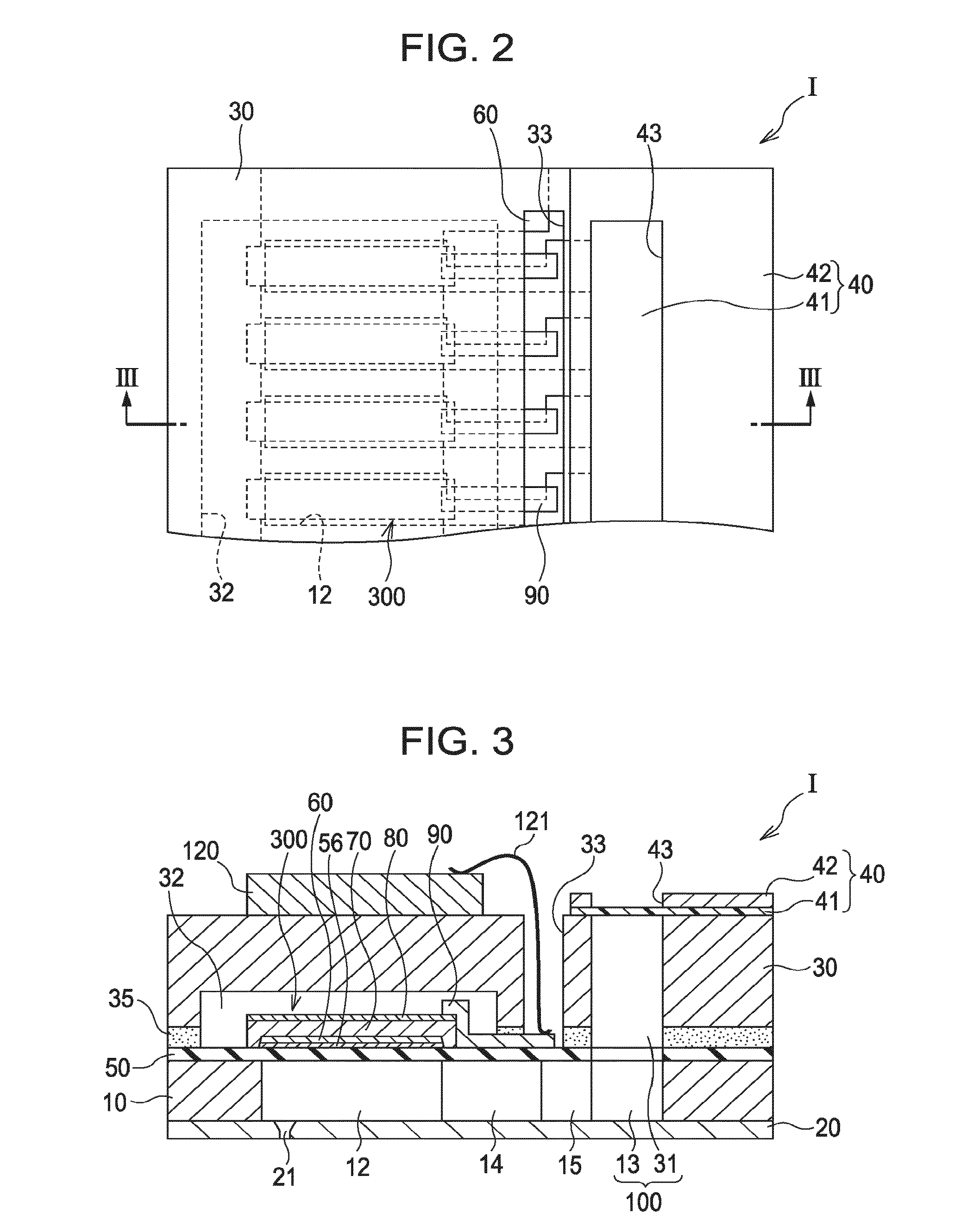
[0027]FIG. 1 is an exploded perspective view schematically illustrating the structure of an ink jet recording head which is one example of a liquid ejecting head according to a first embodiment of the invention. FIG. 2 is a plan view of FIG. 1. FIG. 3 is a cross sectional view along the III-III line of FIG. 2. As illustrated in FIGS. 1 to 3, a flow path formation substrate 10 of this embodiment contains a silicon single crystal substrate, and an elastic film 50 containing silicon dioxide is formed on one surface thereof.
[0028]In the flow path formation substrate 10, a plurality of pressure generating chambers 12 are arranged in parallel in the width direction. Moreover, a communication portion 13 is formed in a region at the outside in the longitudinal direction of the pressure generating chambers 12 of the flow path formation substrate 10, and the communication portion 13 and each pressure generating chamber 12 are made to communicate with each other through an ink supply path 14 a...
example 1
[0066]First, a silicon oxide (SiO2) film was formed on the surface of a single crystal silicon (Si) substrate by thermal oxidation. Next, on the SiO2 film, a zirconium film was produced by sputtering, followed by thermal oxidation, thereby forming a zirconium oxide film. Next, a titanium oxide having a thickness of 40 nm was laminated on the zirconium oxide film, and then a platinum film (first electrode 60) which is oriented in the (111) plane and which has a thickness of 100 nm was formed thereon.
[0067]Subsequently, the piezoelectric layer 70 was formed on the first electrode 60 by spin coating. The technique is as follows. First, n-octane solvent solutions of bismuth 2-ethylhexanoate, iron 2-ethylhexanoate, manganese 2-ethylhexanoate, barium 2-ethylhexanoate, titanium 2-ethylhexanoate, and cerium 2-ethylhexanoate were mixed with a predetermined ratio to thereby prepare a precursor solution.
[0068]Then, the precursor solution was added dropwise on the substrate on which the titaniu...
example 2
[0070]The same operation as in Example 1 was performed, except changing the addition amount of bismuth 2-ethylhexanoate and cerium 2-ethylhexanoate to the precursor solution and forming a piezoelectric material in which Ce / (Ce+Bi) which is a molar ratio of Ce and the total amount of Ce and Bi is 0.05, specifically a complex oxide containing a mixed crystal represented by 0.75[(Bi0.95, Ce0.05) (Fe0.95, Mn0.05)O3]-0.25[BaTiO3] into the piezoelectric layer 70.
PUM
| Property | Measurement | Unit |
|---|---|---|
| molar ratio | aaaaa | aaaaa |
| molar ratio | aaaaa | aaaaa |
| thickness | aaaaa | aaaaa |
Abstract
Description
Claims
Application Information
 - R&D
- Intellectual Property
- Life Sciences
- Materials
- Tech Scout
- Unparalleled Data Quality
- Higher Quality Content
- 60% Fewer Hallucinations
Browse by: Latest US Patents, China's latest patents, Technical Efficacy Thesaurus, Application Domain, Technology Topic, Popular Technical Reports.
© 2025 PatSnap. All rights reserved.Legal|Privacy policy|Modern Slavery Act Transparency Statement|Sitemap|About US| Contact US: help@patsnap.com


