
Optical surface defect inspection apparatus and optical surface defect inspection method

a technology of optical surface defect and inspection apparatus, which is applied in the direction of instruments, measurement devices, scientific instruments, etc., can solve the problem that the autofocus operation cannot physically follow the scan rate, and achieve the effect of improving the signal-to-noise ratio and highly sensitive inspection

Inactive Publication Date: 2013-10-01
HITACHI HIGH-TECH CORP
View PDF5 Cites 0 Cited by
  • Summary
  • Abstract
  • Description
  • Claims
  • Application Information

AI Technical Summary

Benefits of technology

This patent proposes an optical surface defect inspection apparatus and method that can improve the signal-to-noise ratio and implement highly sensitive inspection without autofocus operations. This is achieved by a multi-segmented cell method that allows for efficient detection and analysis of surface defects.

Problems solved by technology

However, in the case where the scan rate is increased excessively, autofocus operations cannot physically follow the scan rate.

Method used


Image

  • Optical surface defect inspection apparatus and optical surface defect inspection method
  • Optical surface defect inspection apparatus and optical surface defect inspection method
  • Optical surface defect inspection apparatus and optical surface defect inspection method

Examples


second embodiment

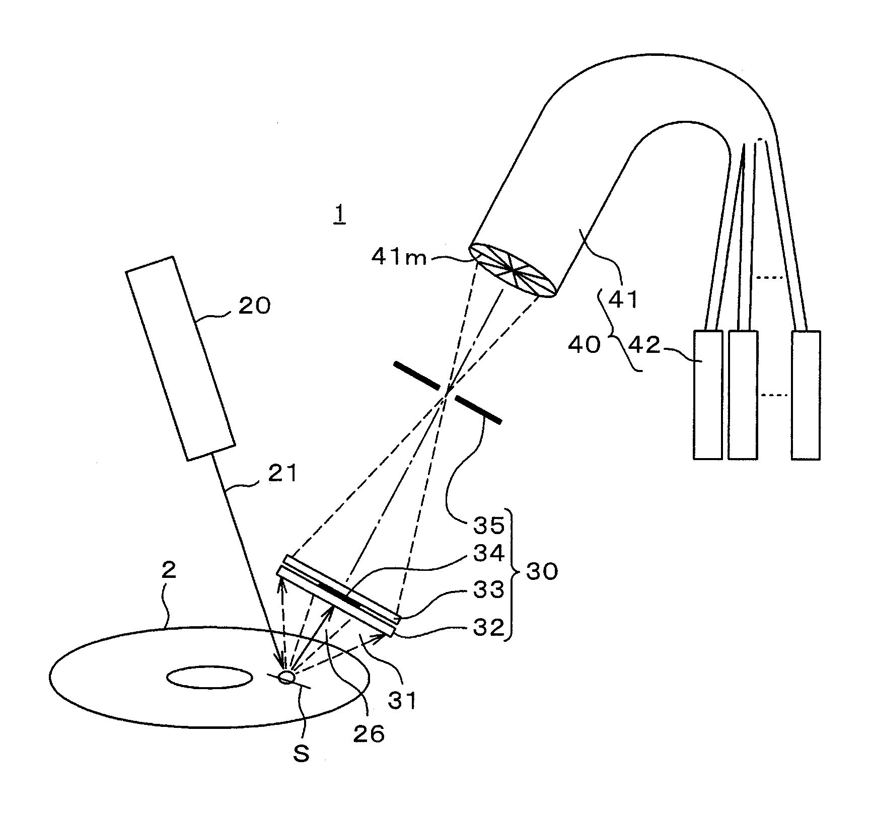
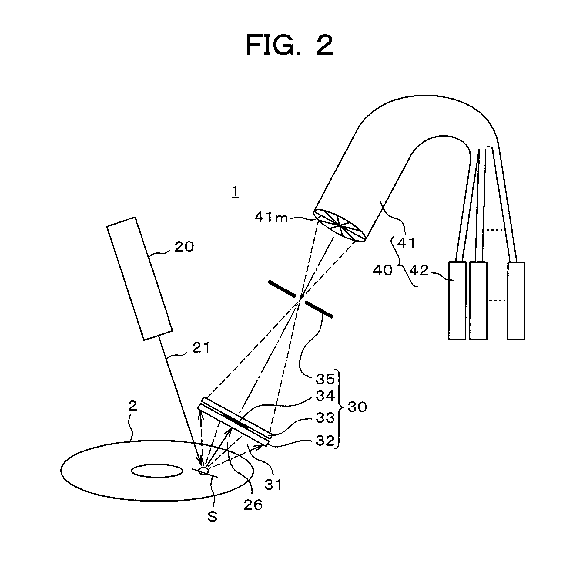
[0030]Of course, as shown in a second embodiment in FIG. 6, it is also possible to separately connect the individual cells A1 to H1 and A2 to H2 to light receiving devices 42A1 to 42H1 and 42A2 to 42H2. In this case, the number of cells divided in the light receiving surface may be an odd number.

[0031]Next, the operation and effect of the inspection optical system 1 described above will be explained.

[0032]Generally, in the case where the surface of the test subject 2 is completely flat like a mirror, the scattered light 31 is rarely produced, and most of the reflected light becomes the positive reflected light 26. On the other hand, in the case where defects such as flaws exist on the surface of the test subject 2, a strong scattered light is produced. This change in the scattered light is captured to detect defects. Moreover, the intensity of scattered light is changed depending on the size or shape of defects.

first embodiment

[0033]When defects on the surface of the test subject are scratches and very shallow flaws, a scattered light to be produced is considerably weak, and it is difficult to distinguish between that scattered light and a scattered light that is background noise produced due to surface roughness or the like. Namely, it is difficult to detect the scattered light because the signal-to-noise ratio is low. For these shallow, scratch-like flaws, the embodiment can improve the signal-to-noise ratio and is effective. In the following, an example will be described in which the light receiving surface 41m is divided into 16 cells, which is an even number (2n), with reference to the first embodiment shown in FIGS. 3 and 5.

[0034]As described above, when the shape of a defect is a line-shaped scratch, such a characteristic is produced that a scattered light is distributed in the direction at a right angle to the orientation of this scratch. On the other hand, a scattered light (background noise) pro...


PUM

PropertyMeasurementUnit
lengthaaaaaaaaaa
center angleaaaaaaaaaa
angleaaaaaaaaaa

Abstract

The present invention is to provide an optical surface defect inspection apparatus or an optical surface defect inspection method that can improve a signal-to-noise ratio according to a multi-segmented cell method without performing autofocus operations, and can implement highly sensitive inspection. The present invention is an optical surface defect inspection apparatus or an optical surface defect inspection method in which an inspection beam is applied onto a test subject, an image of a scattered light from the surface of the test subject is formed on a photo-detector, and a defect on the surface of the test subject is inspected based on an output from the photo-detector. The photo-detector has an optical fiber bundle. One end thereof forms a circular light receiving surface to receive the scattered light. The other end thereof is connected to a plurality of light receiving devices. The optical fiber bundle is divided into a plurality of fan-shaped cells in the light receiving surface, and connected to the light emitting devices in units of the cells for performing the inspection based on the outputs of the plurality of cells.

Description

BACKGROUND OF THE INVENTION[0001]1. Field of the Invention[0002]The present invention relates to an optical surface defect inspection apparatus and an optical surface defect inspection method, and more particularly to an optical surface defect inspection apparatus and an optical surface defect inspection method preferable for use in detecting line-shaped micro defects (scratches) produced on the surface of a test subject.[0003]2. Description of the Related Art[0004]Optical surface defect inspection apparatuses for use in detecting micro defects on the surface of a test subject such as a magnetic disk and an IC wafer are demanded to perform high speed inspection that can meet a 100-percent inspection of the entire surface of all test subjects as well as highly sensitive inspection (detection of micro defects having a width of about a few tens nanometers and a depth of about a few nanometers). Line-shaped micro defects (scratches) considerably damage products particularly, and it is e...

Claims


Application Information

Patent Timeline
Patent Type & Authority Patents(United States)
IPC IPC(8): G01N21/00
CPCG01N21/9501G01N21/9506G01N21/00G01N21/8806G01N2201/0833
Inventor TAMURA, SHINTAROFUKAWA, MASANORIISHIHARA, AYUMUSHITARA, KENICHINAKAJIMA
Owner HITACHI HIGH-TECH CORP
Learn More