Color filter array panel, manufacturing method thereof, and liquid crystal display including the same

a technology of color filter array and manufacturing method, which is applied in the direction of mountings, optics, instruments, etc., can solve the problems of shortening the manufacturing process, and reducing the manufacturing cost, and achieve the effect of simple manufacturing process

Inactive Publication Date: 2013-05-28
SAMSUNG DISPLAY CO LTD
View PDF11 Cites 2 Cited by
  • Summary
  • Abstract
  • Description
  • Claims
  • Application Information

AI Technical Summary

Benefits of technology

[0008]The described technology provides a color filter array panel with a simple manufacturing process, a manufacturing method thereof, and a liquid crystal display including the same.
[0029]According to embodiments of the present invention, the color filter array panel prevents or reduces occurrence of the color filter from being damaged by an etching solution when forming the common cut portion of the common electrode, by filling the protective member in the opening of the color filter.
[0030]Moreover, no separate cover film for protecting the color filter from the etching solution of the common electrode is formed on the color filter, thereby shortening the manufacturing process and reducing manufacturing costs.
[0031]Further, the opening of the color filter and the common cut portion of the common electrode may be formed using the same slit mask, thereby also simplifying the manufacturing process and reducing manufacturing costs.
[0032]In addition, because no separate cover film is formed on the light blocking member, the light blocking member on the periphery of the display panel is brought into direct contact with the sealing material. Accordingly, a release force or bonding force between the thin film transistor array panel and the color filter array panel is improved.
[0033]Additionally, the peripheral cut portion of the common electrode is formed at a position corresponding to the spacer, to bring the spacer into direct contact with the light blocking member, whereby there occurs less or no blurring defect due to applied pressure.

Problems solved by technology

Accordingly, manufacturing costs and time increase.
Moreover, no separate cover film for protecting the color filter from the etching solution of the common electrode is formed on the color filter, thereby shortening the manufacturing process and reducing manufacturing costs.

Method used


Image

  • Color filter array panel, manufacturing method thereof, and liquid crystal display including the same
  • Color filter array panel, manufacturing method thereof, and liquid crystal display including the same
  • Color filter array panel, manufacturing method thereof, and liquid crystal display including the same

Examples


Embodiment Construction

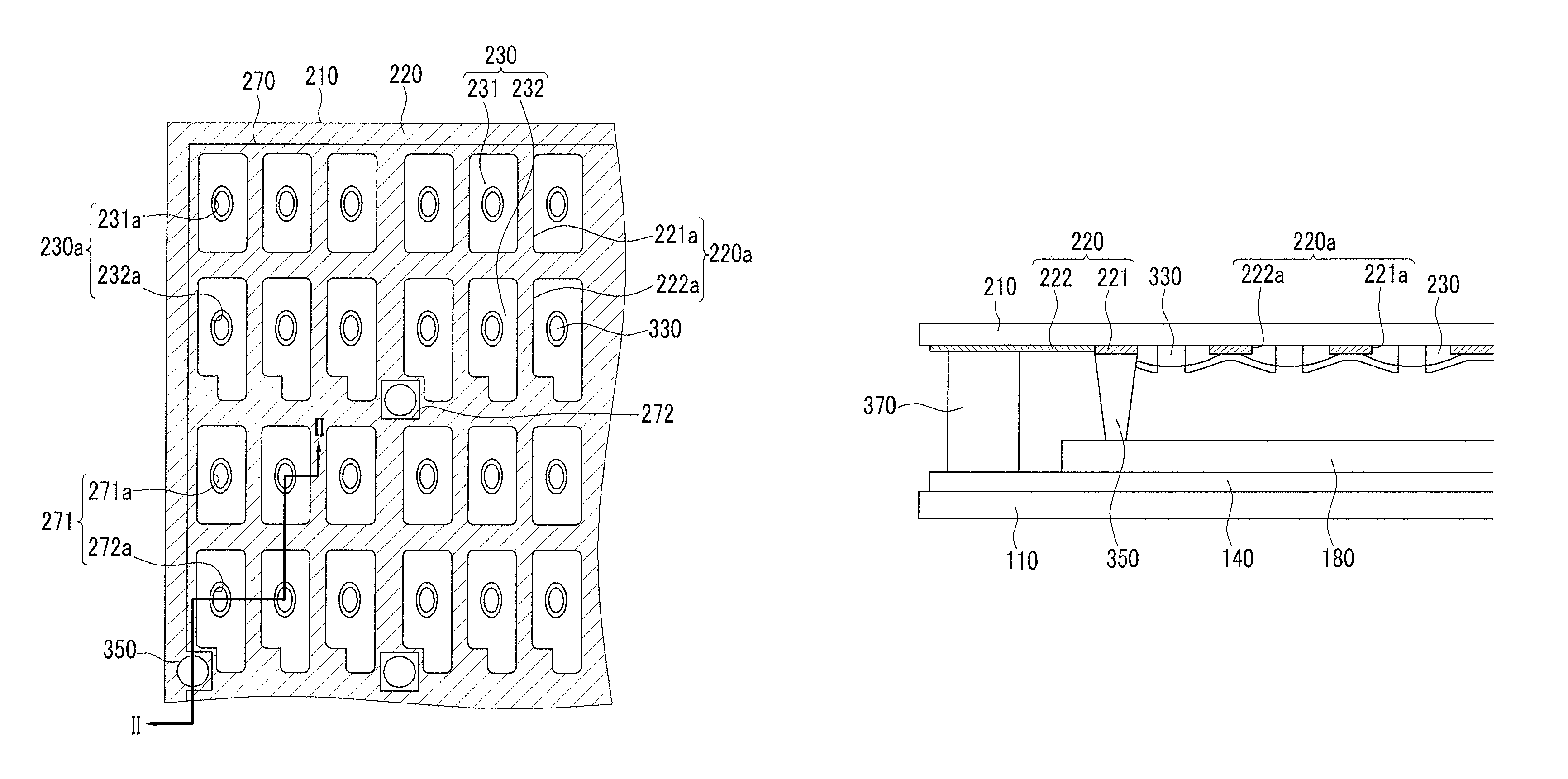
[0042]The present invention will be described more fully hereinafter with reference to the accompanying drawings, in which exemplary embodiments of the invention are shown. As those skilled in the art will recognize, the described embodiments may be modified in various different ways without departing from the spirit or scope of the present invention.

[0043]For various exemplary embodiments, elements having the same or similar constitution are designated with the same reference numerals and explained representatively in the first exemplary embodiment. In other exemplary embodiments, only elements that are different from those in the first exemplary embodiment are described.

[0044]In addition, the size and thickness of each component shown in the drawings are arbitrarily shown for better understanding and ease of description, and thus the present invention is not limited to those properties or characteristics shown in the drawings.

[0045]In the drawings, the thickness of layers, films, ...


PUM

PropertyMeasurementUnit
diameteraaaaaaaaaa
photosensitiveaaaaaaaaaa
sizeaaaaaaaaaa

Abstract

A color filter array panel includes: a substrate; a light blocking member on the substrate; a color filter on the substrate and partially overlapping the light blocking member, and having an opening exposing the substrate; a protective member in the opening; and a common electrode on the light blocking member and the color filter, and having a cut portion at a position corresponding to the opening.

Description

CROSS-REFERENCE TO RELATED APPLICATIONS[0001]This application claims priority to and the benefit of Korean Patent Application No. 10-2010-0041007 filed in the Korean Intellectual Property Office on Apr. 30, 2010, the entire content of which is incorporated herein by reference.BACKGROUND[0002]1. Field[0003]The described technology relates generally to a color filter array panel, a manufacturing method thereof, and a liquid crystal display including the same.[0004]2. Description of Related Art[0005]Liquid crystal displays are one of the most widely used flat panel displays. A liquid crystal display includes two substrates on which electrodes are formed, and a liquid crystal layer that is interposed therebetween, where a voltage is applied to the electrodes to re-arrange liquid crystal molecules of the liquid crystal layer and thereby control the amount of transmitted light.[0006]Small and medium-sized liquid crystal displays of a vertical alignment mode achieve a wide viewing angle by...

Claims


Application Information

Patent Timeline
Patent Type & Authority Patents(United States)
IPC IPC(8): G02F1/1333
CPCG02B5/201G02F1/133509G02F1/133516Y10T29/49002G02F2001/133519G02F2201/50G02F1/133519G02F1/133512G02F1/133555G02F1/13394G02F1/134363G02F1/136227G02F1/136286
Inventor KIM, DONG-GYUKIM, DO-HOON
Owner SAMSUNG DISPLAY CO LTD
Why Eureka
Try Eureka