
MOS solid-state image pickup device

a solid-state image and pickup device technology, applied in the direction of radio control devices, television system scanning details, television systems, etc., can solve the problems of stain-like image defects, achieve the effect of improving the chemical circulation efficiency of the wafer in the spinning off step for spin drying, and preventing the occurrence of stain spots or image defects

Active Publication Date: 2013-04-16
CONVERSANT INTPROP MANAGEMENT INC
View PDF5 Cites 2 Cited by
  • Summary
  • Abstract
  • Description
  • Claims
  • Application Information

AI Technical Summary

Benefits of technology

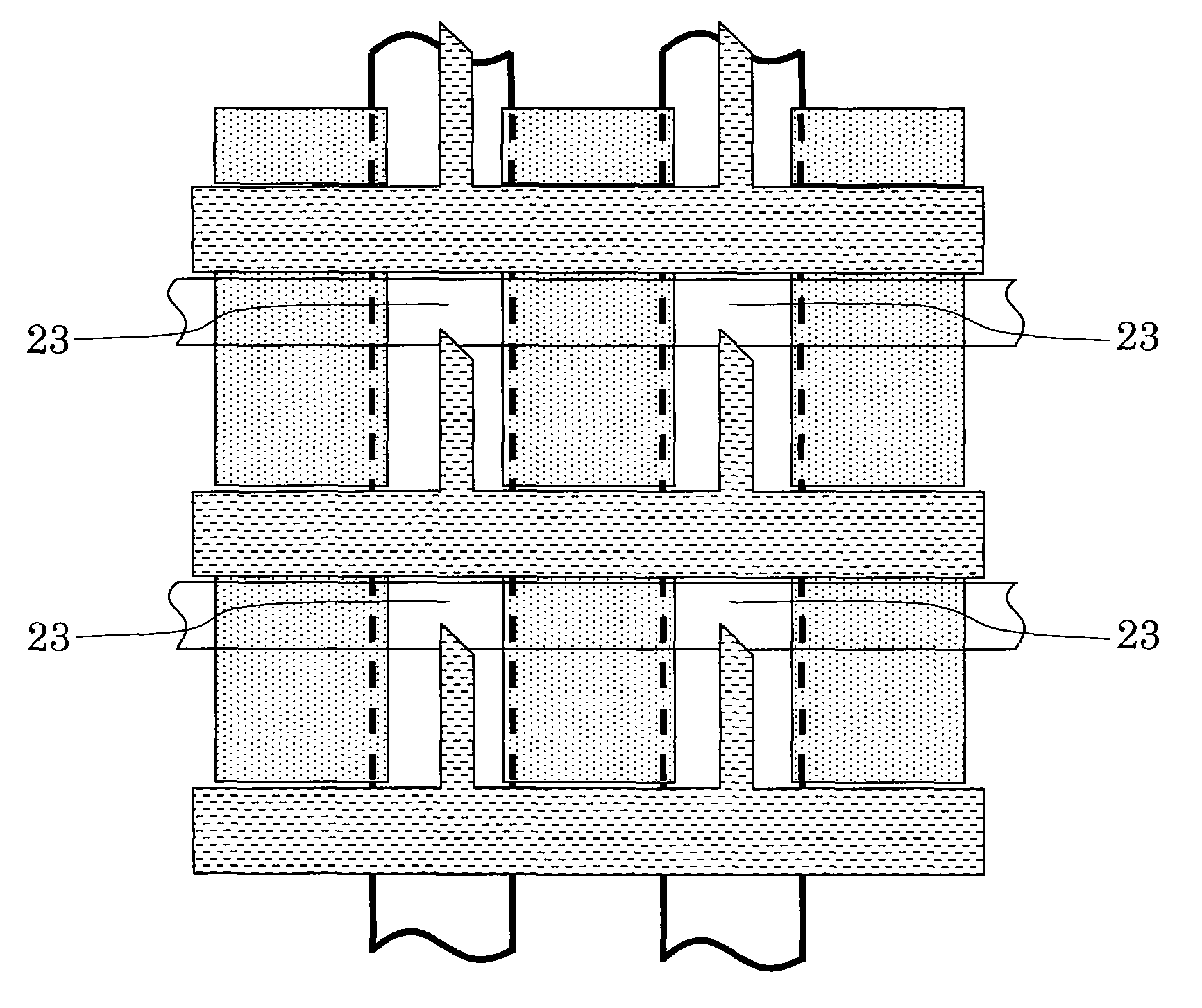
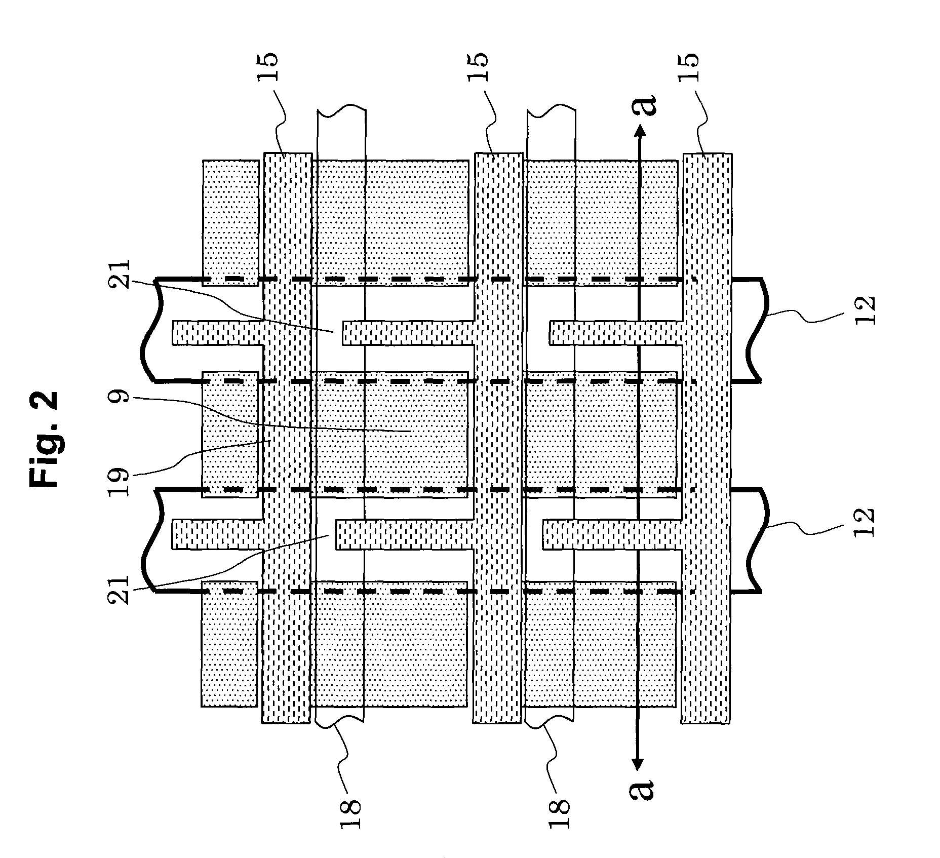
The present invention provides a solid-state image pickup device that prevents stain-like patterns without increasing production cost. This prevents stain spots or image defects and ensures excellent images. The invention uses a gap in a pattern as a discharge port for a chemical reservoir and improves chemical circulation efficiency on the wafer during spin drying, preventing uneven etching in an interlayer insulating film above the light reception region.

Problems solved by technology

A problem was found that stain-like image defects occur in the process of forming the light blocking film having a lattice pattern.

Method used


Image

  • MOS solid-state image pickup device
  • MOS solid-state image pickup device
  • MOS solid-state image pickup device

Examples


Embodiment Construction

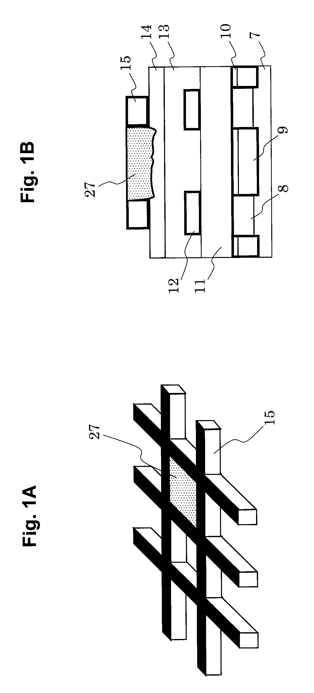
[0031]The inventors of the present invention further reviewed a cause of stain pattern in the pixel cell array region of a solid-state image pickup device. FIG. 1A is a perspective view of a light blocking film and FIG. 1B is a cross-sectional view of a pixel cell part of a solid-state image pickup device. A basic structure will be described with reference to FIG. 1B. On an N-type silicon substrate 7, an element separation film 8 is formed, a two-dimensional array of multiple photodiodes 9 is provided, and a P-type surface shielding layer 10 is provided thereon. Above them, a first interlayer insulating film 11, a first wiring layer 12, a second interlayer insulating film 13, a fluorine diffusion inhibiting film 14 and a second wiring layer 15 are further formed. FSG (fluorinated silicate glass) is sometime used for the second interlayer insulating layer 13 and, therefore, a p-SiON film 14 is used as the fluorine diffusion inhibiting film 14.

[0032]Both the first wiring layer 12 and ...


PUM


Abstract

A solid-state image pickup device relating to the present invention has a specific gap in a part of a lattice-shaped light blocking film pattern or wiring pattern having an opening enclosing a light reception region. Peripheral circuits and wiring layers on a pixel may be used as the light blocking film. In such a case, when multiple wiring layers are used as the light blocking film, layouts of a second and subsequent wiring layers is determined according to the layout of the first wiring layer above the light reception region. The specific gap is created in a part of the wiring enclosing the light reception region.

Description

CROSS-REFERENCE TO RELATED APPLICATION[0001]The disclosure of Japanese Patent Application No. 2008-247611 filed Sep. 26, 2008 including specification, drawings and claims is incorporated herein by reference in its entirety.BACKGROUND OF THE INVENTION[0002]1. Field of the Invention[0003]The present invention relates to a technique to obtain excellent images free from image defects such as stain spots without increasing process cost in a solid-state image pickup device such as a CCD (charger coupled device) or MOS (metal oxide semiconductor) image sensor having photoelectric conversion elements on a semiconductor substrate.[0004]2. Description of the Related Art[0005]The CCD image sensor as a solid-state image pickup device has photoelectric conversion elements, such as photodiodes, and a charge transfer path on a semiconductor substrate, wherein light emitted on the photoelectric conversion elements is converted to signal charge. The signal charge is transferred through the charge tr...

Claims


Application Information

Patent Timeline
Patent Type & Authority Patents(United States)
IPC IPC(8): H01L27/146H01L27/14H01L31/10
CPCH01L27/14623H01L27/14645
Inventor MIMURO, KENJISAKI, JUN
Owner CONVERSANT INTPROP MANAGEMENT INC
Learn More