
Non-volatile memory device and method for controlling the same

a non-volatile memory and memory device technology, applied in static storage, digital storage, instruments, etc., can solve the problems of invariable shape of p(i) distribution, slow operating speed, and conventional flash memory devices, so as to improve the operation margin of non-volatile memory devices, increase operation reliability, and prevent a faulty operation

Active Publication Date: 2013-03-19
SK HYNIX INC
View PDF5 Cites 5 Cited by
  • Summary
  • Abstract
  • Description
  • Claims
  • Application Information

AI Technical Summary

Benefits of technology

[0040]Third, an embodiment of the present invention relates to a non-volatile memory device for generating a global reference current varying in response to an operation environment of a unit cell array, thereby improving an operation margin of the non-volatile memory device.
[0041]Fourth, an embodiment of the present invention relates to a non-volatile memory device for substantially preventing a faulty operation from being generated in a read operation, resulting in the increased operation reliability.

Problems solved by technology

Although a NOR flash memory device or a NAND flash memory device has been widely used as non-volatile memory, a conventional flash memory device has a disadvantage in that it has a slow operating speed.
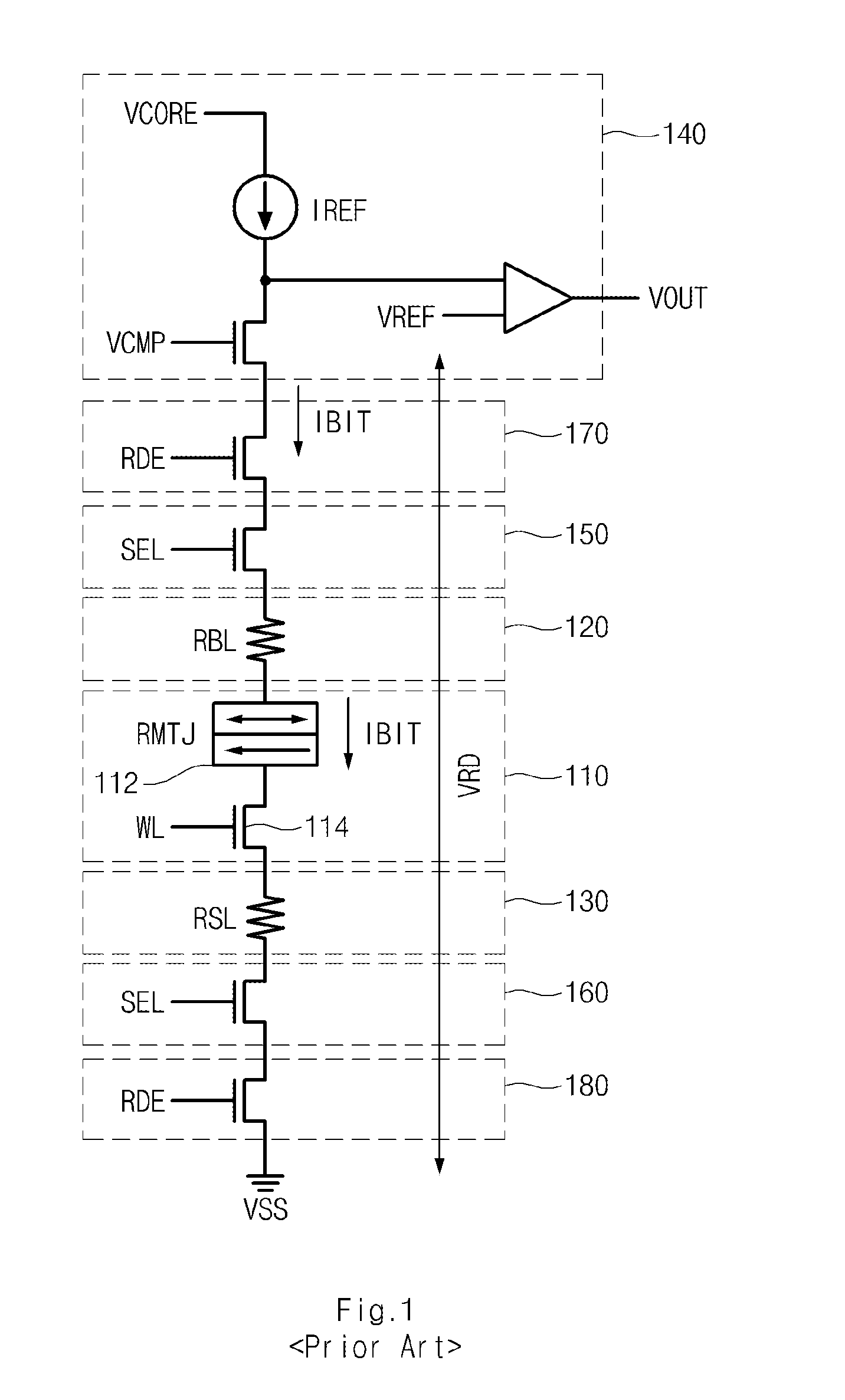
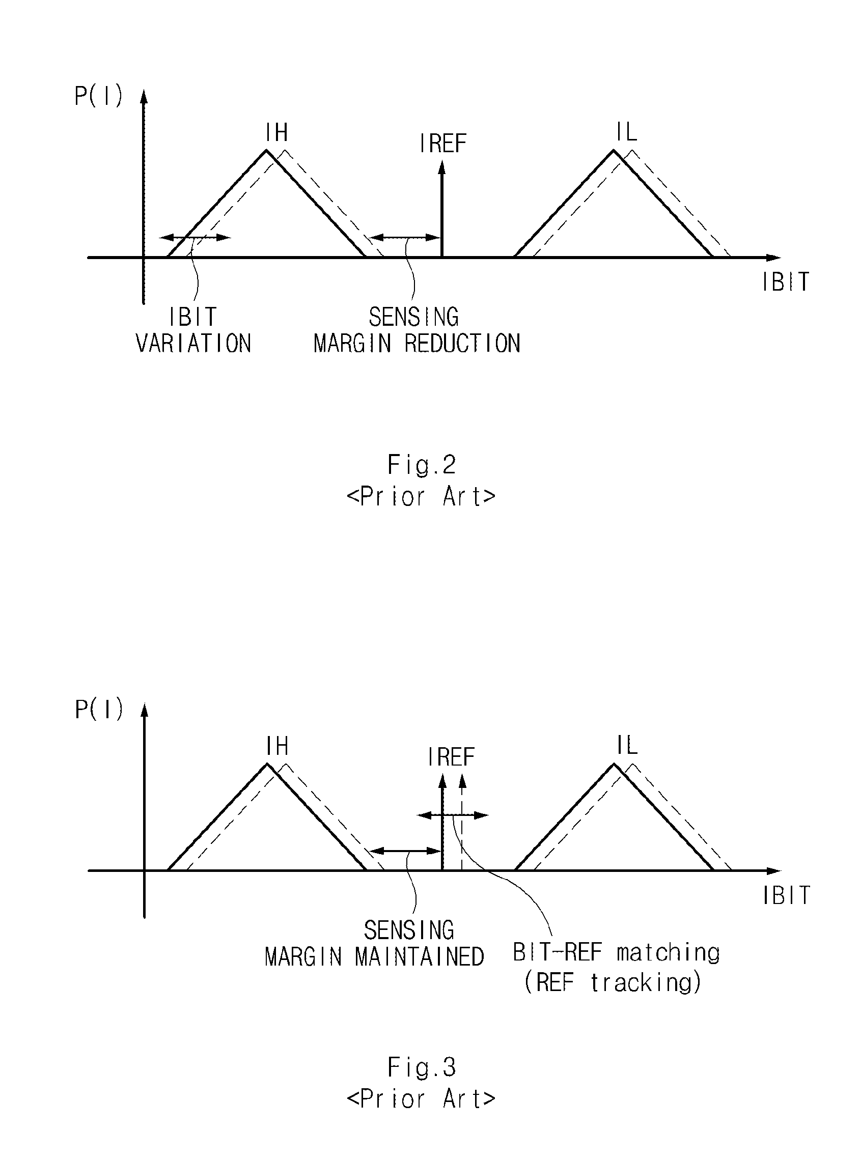
However, it should be noted that the P(I) distribution is not always maintained in an invariable shape.
If worst comes to worst, a faulty operation in which data is incorrectly sensed may be generated.
However, in the relative reference current scheme, both the area of a circuit generating the reference current IREF and power consumption are increased so as to change the reference current IREF.

Method used


Image

  • Non-volatile memory device and method for controlling the same
  • Non-volatile memory device and method for controlling the same
  • Non-volatile memory device and method for controlling the same

Examples


Embodiment Construction

[0057]Reference will now be made in detail to the embodiments of the present invention, examples of which are illustrated in the accompanying drawings. Wherever possible, the same reference numbers will be used throughout the drawings to refer to the same or like parts.

[0058]In order to guarantee a margin for a stable read operation in a non-volatile memory device operating in a low-power environment, an embodiment of the present invention corrects a variation of a resistance value generated in a read path for data transmission according to an operation environment and a reference cell position, such that data can be definitely identified even though the intensity of a signal corresponding to data is very low.

[0059]FIG. 4 is a circuit diagram illustrating a non-volatile memory device for implementing a relative reference current scheme.

[0060]Referring to FIG. 4, the non-volatile memory device includes a unit cell 410, a bit line 420, a source line 430, a sense-amp 440, a first switc...


PUM


Abstract

A non-volatile memory and method for controlling the same prevents a faulty operation from being generated in a read operation, resulting in increase in operation reliability. The non-volatile memory device includes a cell array configured to include a plurality of unit cells in which a read or write operation of data is achieved in a unit cell in response to a variation of resistance, a reference cell array configured to include a plurality of reference cells, each of which has the same structure as that of the unit cell, a global reference current generation circuit configured to generate a global reference current corresponding to a position of the reference cell so as to verify data stored in the reference cell array, and a sense-amplifier configured to compare a current flowing in the reference cell array with the global reference current during a write verification operation of the reference cell array, and thus sense data.

Description

CROSS-REFERENCE TO RELATED APPLICATION[0001]The priority of Korean patent application No. 10-2010-0124843 filed on Dec. 8, 2010, the disclosure of which is hereby incorporated in its entirety by reference, is claimed.BACKGROUND OF THE INVENTION[0002]Embodiments of the present invention relate to a non-volatile memory device and method for controlling the same, and more specifically, to a technology for increasing the operation reliability of a non-volatile memory device in such a manner that the sensing and transmitting of data can be stably achieved during a read operation in which data stored in a unit cell is output externally.[0003]Semiconductor memory devices have been rapidly developed to temporarily or permanently store data therein. The semiconductor memory devices have been widely used in a variety of electronic appliances, electronic devices, and personal portable devices. General semiconductor memory devices can freely read and / or write data, and can also easily update ol...

Claims


Application Information

Patent Timeline
Patent Type & Authority Patents(United States)
IPC IPC(8): G11C11/00
CPCG11C11/15G11C11/1673G11C11/1697
Inventor RHO, KWANG MYOUNG
Owner SK HYNIX INC
Learn More