Eureka AIR delivers breakthrough ideas for toughest innovation challenges, trusted by R&D personnel around the world.

Cyclical epitaxial deposition and etch

a technology of epitaxial growth and etching, which is applied in the direction of basic electric elements, electrical equipment, semiconductor devices, etc., can solve the problems of low quality epitaxial growth and often poor growth quality

Active Publication Date: 2013-02-05
ASM IP HLDG BV
View PDF307 Cites 439 Cited by
  • Summary
  • Abstract
  • Description
  • Claims
  • Application Information

AI Technical Summary

Benefits of technology

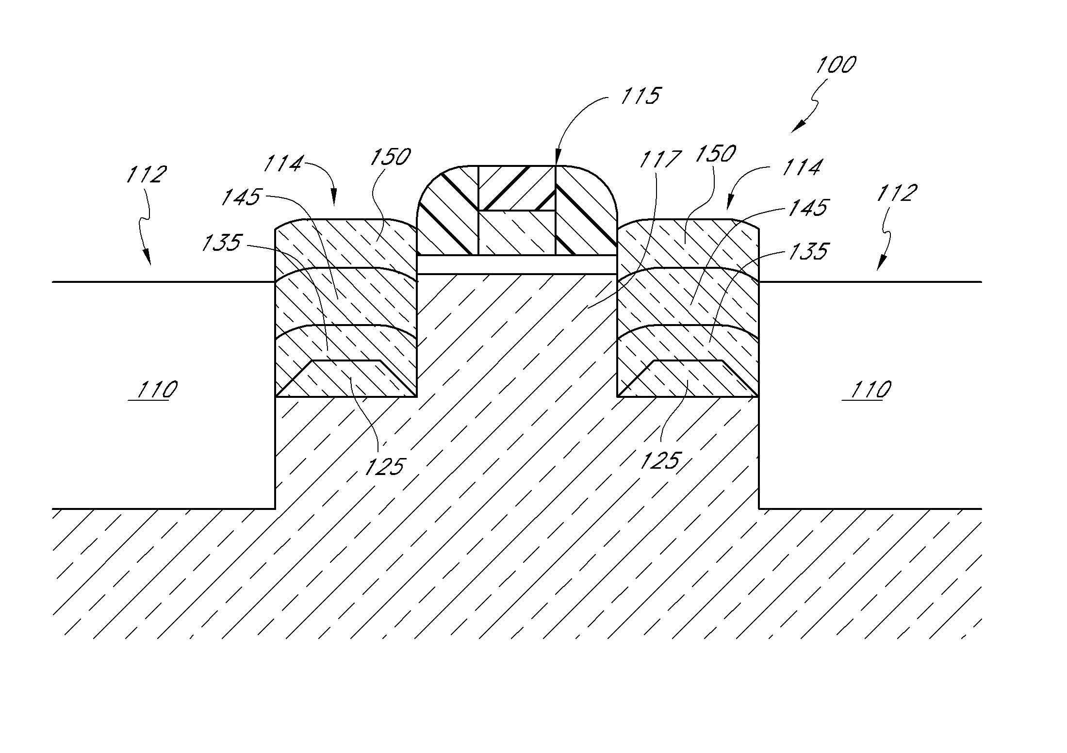
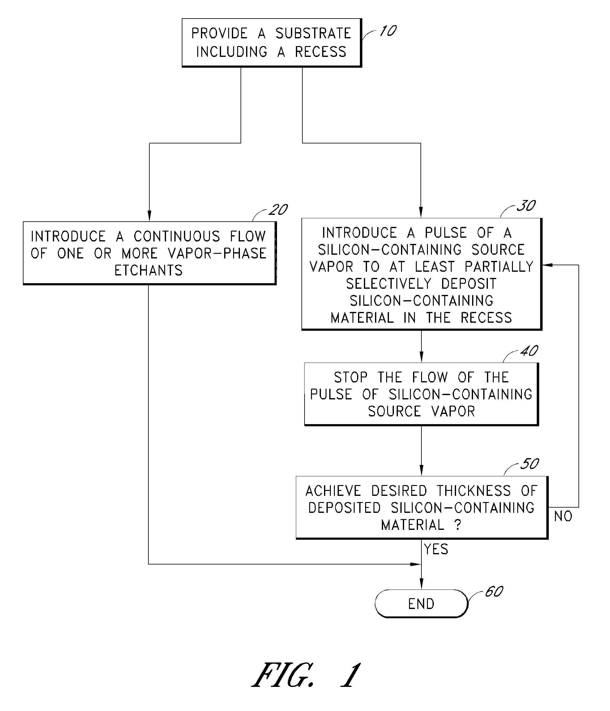
[0009]The present application describes methods of cyclical epitaxial deposition and etch. Some embodiments can provide for bottom-up growth of epitaxial material that is of high quality.

Problems solved by technology

However, while known processes often result in selective epitaxial growth, such growth is often of poor quality.
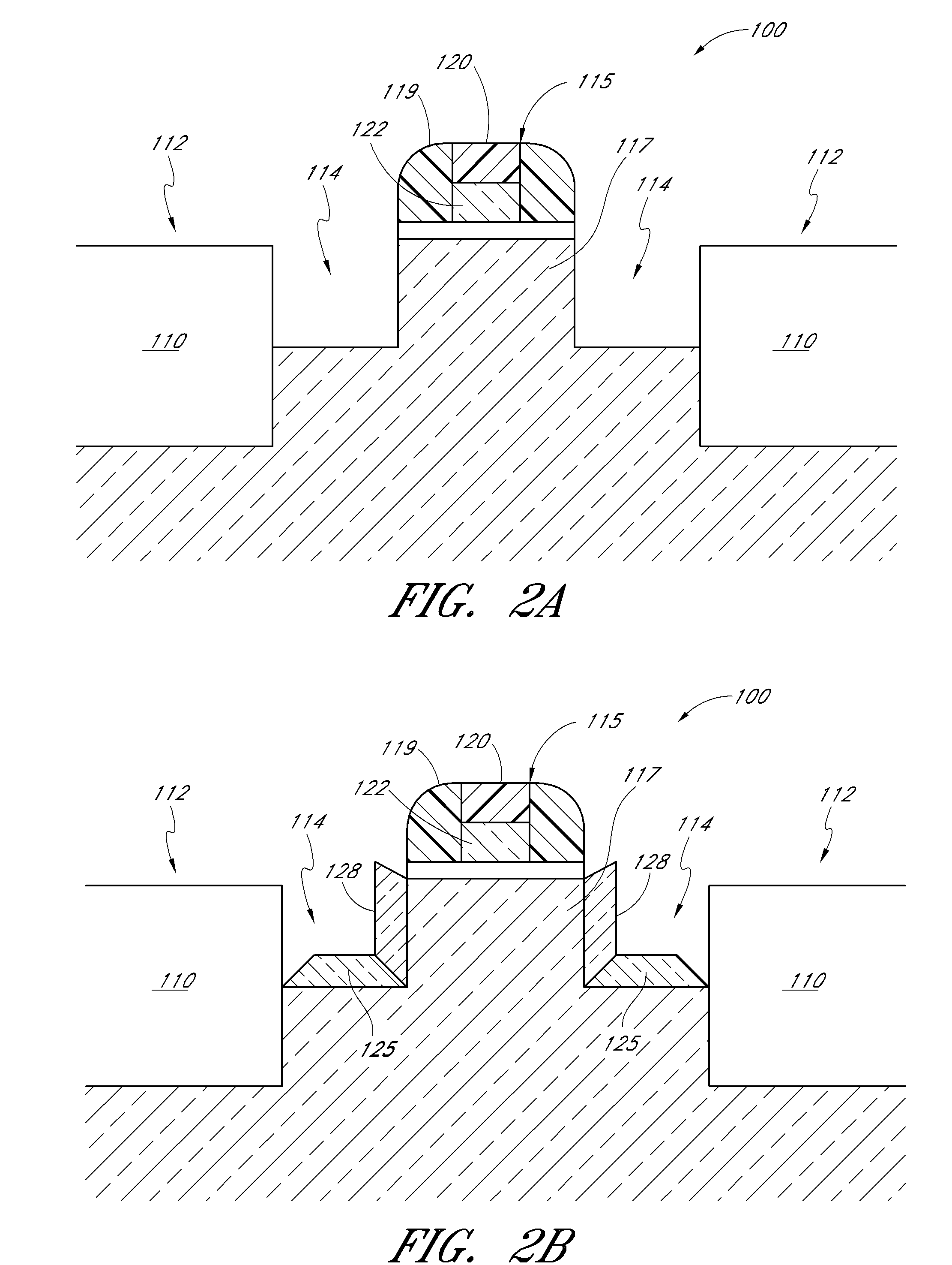
For example, in current processes that provide selective growth in source / drain recesses, pronounced crystallographic defects may often originate in the bottom corner and sidewalls of the recess areas, resulting in undesirable, low quality epitaxial growth.

Method used


Image

  • Cyclical epitaxial deposition and etch
  • Cyclical epitaxial deposition and etch
  • Cyclical epitaxial deposition and etch

Examples


example process

PARAMETERS

Example 1

[0071]Example process parameters are summarized in Table A below, which lists operating ranges for a selective deposition process according to one embodiment using either Cl2 or HCl as an etchant gas. Optional ranges are provided in parentheses. As is evident from Table A, the process conditions such as chamber temperature, chamber pressure and carrier gas flow rates, are preferably substantially similar throughout the selective deposition process, thereby allowing throughput to be increased. Thus, the example below employs isothermal and isobaric conditions during the selective formation process.

[0072]

TABLE AProcess PhasePre-SelectiveTransition Period toPost-EtchDepositionEpitaxialSelective EpitaxialPurge(one time atGrowthEtchGrowth (SEG);(one time atbeginning)(SEG)Backrepeat x-timesend)duration (sec)52.4-12 2.4-30 .1 s10temp (° C.)525-600 525-600 525-600 525-600 525-600 pressure (Torr)10-20010-20010-20010-20010-200H2 / He flow (slm)2-202-202-202-202-20Cl2 / HCl flow...

example 2

[0078]Example process parameters are summarized in Table B below, which lists operating ranges for a selective deposition process according to one embodiment using HCl as an etchant gas. Optional ranges are provided in parentheses. As is evident from Table B, the process conditions such as chamber temperature and chamber pressure, are preferably substantially similar throughout the selective deposition process, thereby allowing throughput to be increased. Thus, the example below employs isothermal and isobaric conditions during the selective formation process.

[0079]

TABLE BTransitionPre-Period toDepositionDeposition(once at(repeat 30beginning)DepositionPurge 1Purge 2EtchPurge 3Purge 4times)Time303.63.62.463.62.40.1[s]PurposeSiCP(Ge)Purge outRamp downEtch Ge withRamp updepSi3H8, MMS,Hehigh HCL / lowHePH3HeTokenDepDepDepDepDepDepDepDepTemp525525525525525525525525[° C.]Pressure200200200200200200200200[Torr]He [slm]1010102221010Si3H8100V100———100V100V100V[mg / min]MMS60V6060V60V60V60V6060[sc...


PUM

PropertyMeasurementUnit
pressureaaaaaaaaaa
pressureaaaaaaaaaa
pressureaaaaaaaaaa

Abstract

Methods for selectively depositing high quality epitaxial material include introducing pulses of a silicon-source containing vapor while maintaining a continuous etchant flow. Epitaxial material is deposited on areas of a substrate, such as source and drain recesses. Between pulses, the etchant flow continues such that lower quality epitaxial material may be removed, as well as any non-epitaxial material that may have been deposited. The pulse of silicon-source containing vapor may be repeated until a desired thickness of epitaxial material is selectively achieved in semiconductor windows, such as recessed source / drain regions.

Description

BACKGROUND OF THE INVENTION[0001]1. Field of the Invention[0002]The present application relates to methods of epitaxial deposition of silicon-containing materials. More specifically, the present application relates to methods of cyclical epitaxial deposition and etch.[0003]2. Description of the Related Art[0004]Semiconductor processing is typically used in the fabrication of integrated circuits, which entails particularly stringent quality demands. A variety of methods are used in the semiconductor manufacturing industry to deposit material onto surfaces. One of the most widely used methods is chemical vapor deposition (“CVD”), in which atoms or molecules contained in a vapor deposit on a surface to form a film. CVD allows for the growth of films on device surface areas, including “epitaxial” films comprised of a crystalline silicon-containing material.[0005]In some applications it may be desirable to achieve uniform or “blanket” deposition of epitaxial growth over mixed surfaces, s...

Claims


Application Information

Patent Timeline
Patent Type & Authority Patents(United States)
IPC IPC(8): H01L21/20
CPCH01L21/02381H01L21/0243H01L21/02433H01L21/02532H01L21/02573H01L21/0262H01L21/02639H01L29/0847H01L29/66628H01L29/66636H01L29/7848
Inventor BAUER, MATTHIASTHOMAS, SHAWN G.
Owner ASM IP HLDG BV
Why Eureka
Eureka Blog
Learn More