
Semiconductor device and method for manufacturing the same

a technology of semiconductors and semiconductors, applied in semiconductor devices, electrical equipment, transistors, etc., can solve the problems of taking an enormous amount of time to form thin film transistors using polycrystalline silicon, and achieve the effects of preventing change in composition or deterioration in film quality, and reducing the cost of production

Active Publication Date: 2013-01-01
SEMICON ENERGY LAB CO LTD
View PDF164 Cites 77 Cited by
  • Summary
  • Abstract
  • Description
  • Claims
  • Application Information

AI Technical Summary

Benefits of technology

The present invention provides a thin film transistor with a protective layer made of a second oxide semiconductor region between the first oxide semiconductor region and a protective insulating layer, which prevents change in composition or deterioration in film quality of the first oxide semiconductor region and stabilizes electrical characteristics of the thin film transistor. This results in a display device with high electrical characteristics and reliability.

Problems solved by technology

On the other hand, although a thin film transistor using polycrystalline silicon has high field effect mobility, it takes an enormous amount of time to form the thin film transistor using polycrystalline silicon over a large-sized substrate such as a large glass substrate because a crystallization process such as laser annealing is needed.

Method used


Image

  • Semiconductor device and method for manufacturing the same
  • Semiconductor device and method for manufacturing the same
  • Semiconductor device and method for manufacturing the same

Examples


embodiment 1

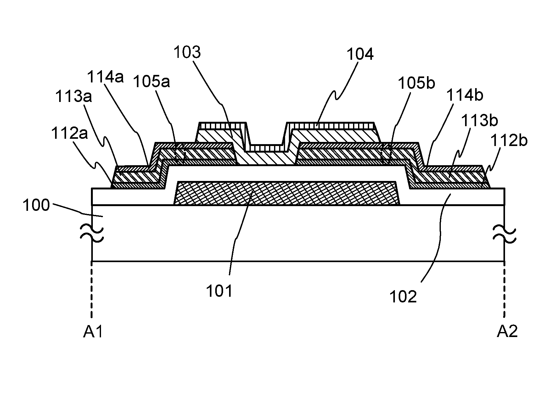
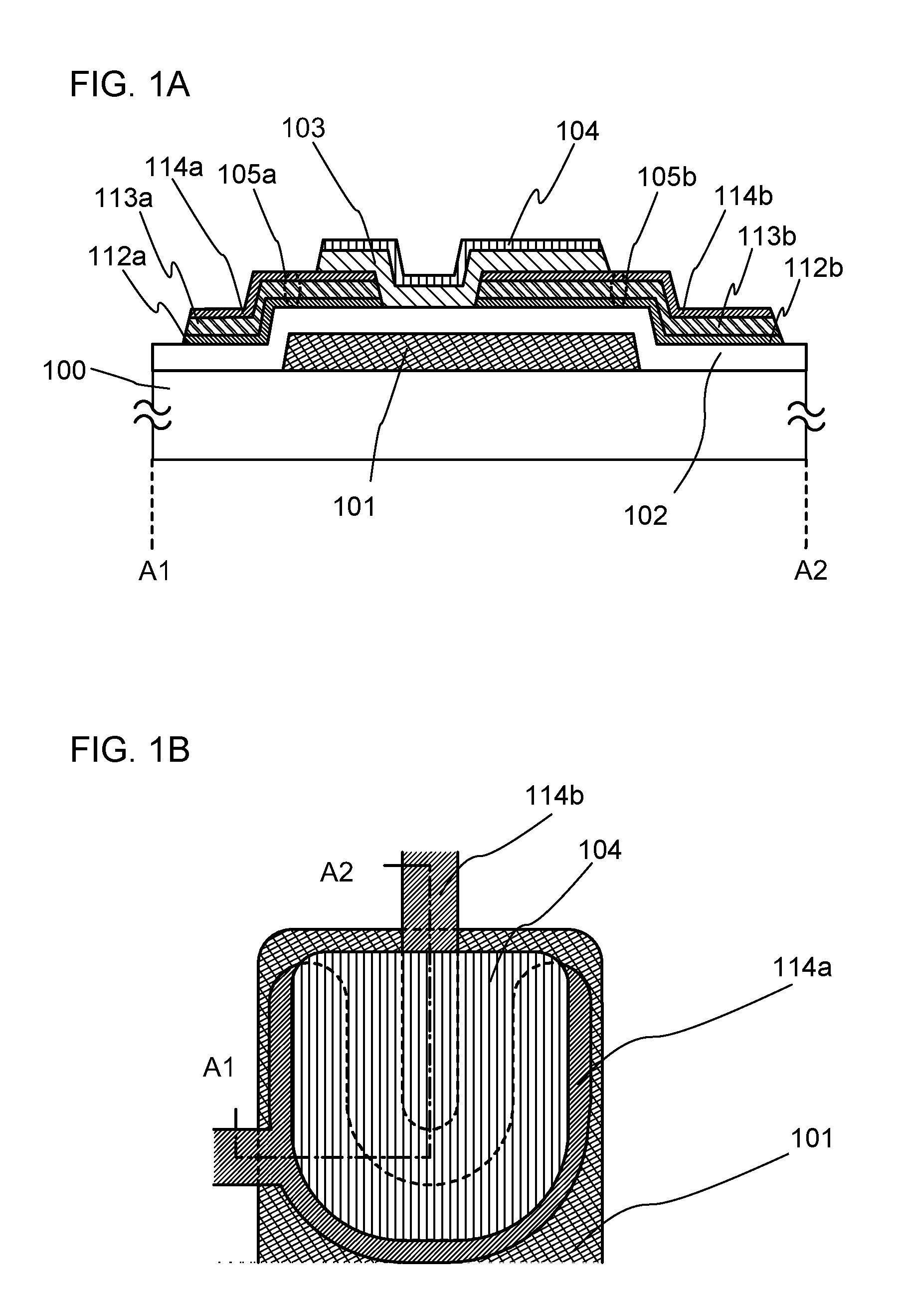
[0059]In this embodiment, a structure of a thin film transistor is described with reference to FIGS. 1A and 1B.

[0060]A thin film transistor having a bottom gate structure of this embodiment is illustrated in FIGS. 1A and 1B. FIG. 1A is a cross-sectional view, and FIG. 1B is a plan view. FIG. 1A is a cross-sectional view along line A1-A2 of FIG. 1B.

[0061]In the thin film transistor illustrated in FIGS. 1A and 1B, a gate electrode layer 101 is provided over a substrate 100, a gate insulating layer 102 is provided over the gate electrode layer 101, a source and drain electrode layers 105a and 105b are provided over the gate insulating layer 102, a first oxide semiconductor region 103 is provided over the gate insulating layer 102 and the source and drain electrode layers 105a and 105b, and a second oxide semiconductor region 104 having lower electrical conductivity than the first oxide semiconductor region 103 is provided over the first oxide semiconductor region 103. Note that the fir...

embodiment 2

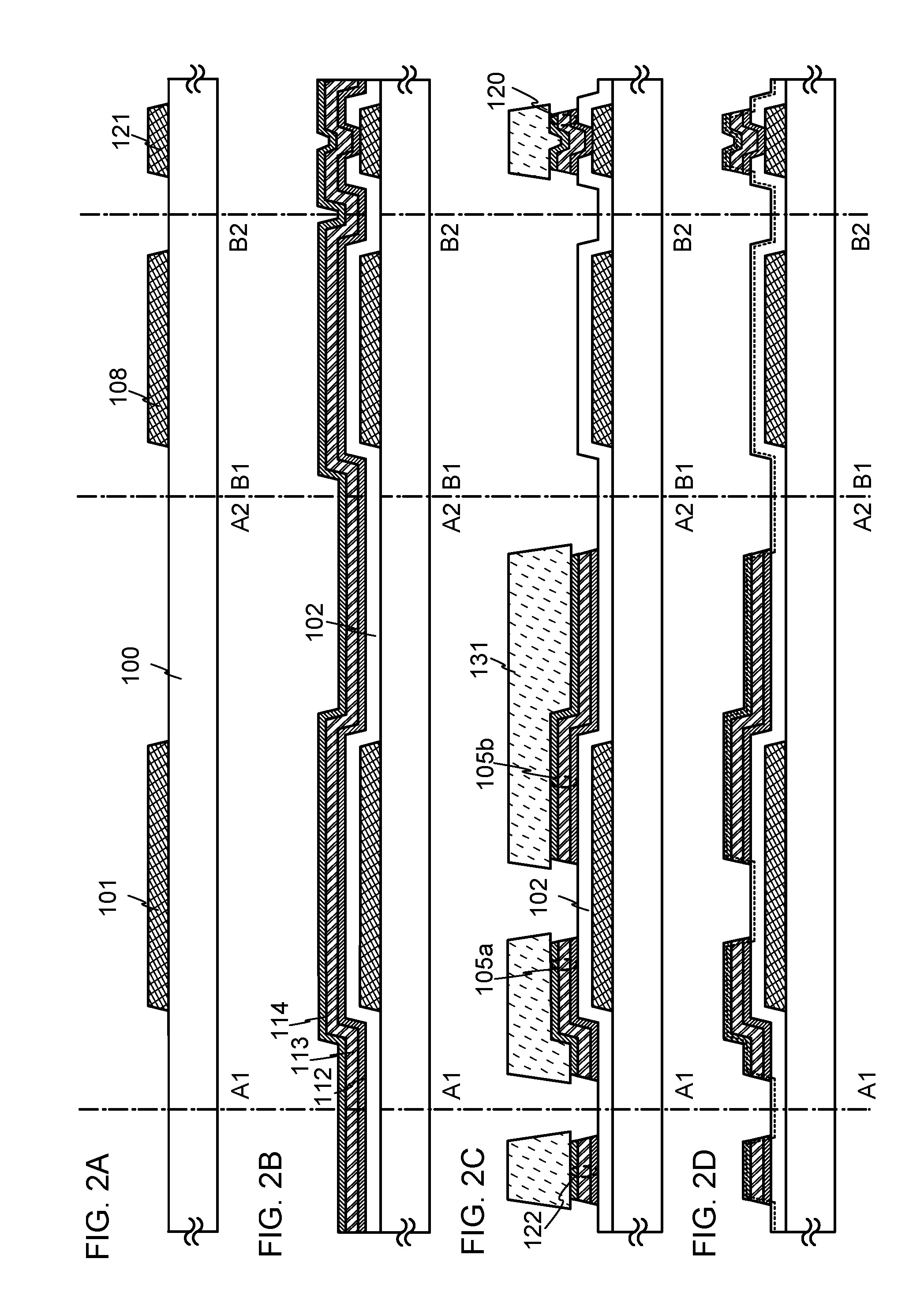
[0081]In this embodiment, a manufacturing process of a display device including the thin film transistor described in Embodiment 1 will be described with reference to FIGS. 2A to 2D, FIGS. 3A to 3C, FIG. 4, FIG. 5, FIG. 6, FIG. 7, FIGS. 8A-1, 8A-2, 8B-1, and 8B-2, and FIG. 9. FIGS. 2A to 2D and FIGS. 3A to 3C are cross-sectional views, and FIG. 4, FIG. 5, FIG. 6, and FIG. 7 are plan views. Line A1-A2 and line B1-B2 in each of FIG. 4, FIG. 5, FIG. 6, and FIG. 7 correspond to line A1-A2 and line B1-B2 in each of the cross-sectional views of FIGS. 2A to 2D and FIGS. 3A to 3C, respectively.

[0082]First, the substrate 100 is prepared. As the substrate 100, any of the following substrates can be used: non-alkaline glass substrates made of barium borosilicate glass, aluminoborosilicate glass, aluminosilicate glass, and the like by a fusion method or a float method; ceramic substrates; plastic substrates having heat resistance enough to withstand a process temperature of this manufacturing p...

embodiment 3

[0138]In this embodiment, a thin film transistor having a different structure than that of the thin film transistor described in Embodiment 1 is described with reference to FIG. 10.

[0139]A thin film transistor having a bottom gate structure of this embodiment is illustrated in FIG. 10. In the thin film transistor illustrated in FIG. 10, the gate electrode layer 101 is provided over the substrate 100, the gate insulating layer 102 is provided over the gate electrode layer 101, the source and drain electrode layers 105a and 105b are provided over the gate insulating layer 102, buffer layers 301a and 301b are provided over the source and drain electrode layers 105a and 105b, the first oxide semiconductor region 103 is provided over the gate insulating layer 102 and the buffer layers 301a and 301b, and the second oxide semiconductor region 104 having lower electrical conductivity than the first oxide semiconductor region 103 is provided over the first oxide semiconductor region 103. Not...


PUM


Abstract

An object is, in a thin film transistor in which an oxide semiconductor is used as an active layer, to prevent change in composition, film quality, an interface, or the like of an oxide semiconductor region serving as an active layer, and to stabilize electrical characteristics of the thin film transistor. In a thin film transistor in which a first oxide semiconductor region is used as an active layer, a second oxide semiconductor region having lower electrical conductivity than the first oxide semiconductor region is formed between the first oxide semiconductor region and a protective insulating layer for the thin film transistor, whereby the second oxide semiconductor region serves as a protective layer for the first oxide semiconductor region; thus, change in composition or deterioration in film quality of the first oxide semiconductor region can be prevented, and electrical characteristics of the thin film transistor can be stabilized.

Description

BACKGROUND OF THE INVENTION[0001]1. Field of the Invention[0002]The present invention relates to a semiconductor device using an oxide semiconductor, a display device using the semiconductor device, and a manufacturing method thereof.[0003]2. Description of the Related Art[0004]In recent years, liquid crystal display devices typified by liquid crystal displays are becoming widespread. As a liquid crystal display, an active matrix liquid crystal display device provided with pixels each including a thin film transistor (TFT) is often used. In a thin film transistor included in an active matrix liquid crystal display device, amorphous silicon or polycrystalline silicon is used as an active layer. Although a thin film transistor using amorphous silicon has low field effect mobility, it can be easily formed over a large-sized substrate such as a large glass substrate. On the other hand, although a thin film transistor using polycrystalline silicon has high field effect mobility, it takes...

Claims


Application Information

Patent Timeline
Patent Type & Authority Patents(United States)
IPC IPC(8): H01L27/14H01L21/00
CPCH01L21/02554H01L21/02565H01L21/02631H01L29/45H01L29/66742H01L29/7869H01L29/78696H01L29/66969H01L29/786H01L29/78606H01L27/1225H01L21/82H01L29/0684H01L29/24H01L29/06H01L29/78693
Inventor AKIMOTO, KENGOSASAKI, TOSHINARIKUWABARA, HIDEAKI
Owner SEMICON ENERGY LAB CO LTD
Learn More