
Probe assembly and manufacturing method thereof

a technology of probe pins and assembly methods, applied in the direction of electronic circuit testing, measurement devices, instruments, etc., can solve the problems of difficult to precisely dispose of pins with a high level of coplanarity, difficult to arrange the probe pins without electrical and mechanical interference between adjacent pins, and high cost, so as to achieve convenient and reliable disposed, easy to arrange, and small pitch

Inactive Publication Date: 2012-12-11
LEE JAE HA
View PDF9 Cites 1 Cited by
  • Summary
  • Abstract
  • Description
  • Claims
  • Application Information

AI Technical Summary

Benefits of technology

[0031]According to the present invention, the insertion holes of the base layer are formed respectively corresponding to the pads of the circuit board and the probe pins are firmly fixed through the conductive adhesive filled in the insertion holes. By using the insertion holes, the probe pins can be easily arranged with small pitch and respectively reliably disposed without mechanically electrically interfering with neighboring pins because neighboring insertion holes provide spaces completely separated from each other. Furthermore, the areas of the insertion holes are sufficiently larger than the probe pins inserted thereinto, and thus the conductive adhesive can completely fill the insertion holes and fully envelope the probe pins to firmly support the probe pins. In addition, the method for manufacturing a probe assembly using insertion holes can easily manufacture a probe assembly at a reduced manufacturing cost.
[0032]Moreover, during a process of manufacturing a probe assembly, the probe pins can be vertically aligned through the flat surface of the first aligning mask layer to secure good coplanarity. Furthermore, the probe pins can be precisely aligned in the horizontal direction through aligning holes of the second aligning mask layer or aligning holes or aligning recesses of the aligning mask.
[0033]In addition, the base layer into which the probe pins are inserted and fixed is formed of the same semiconductor material as a water to be tested such that the base layer and the wafer have the same coefficient of thermal expansion. Accordingly, it is possible to solve the conventional problem that the probe pins deviate from the contact pads on the wafer during a hot test or a cold test due to a difference in the coefficient of thermal expansion between the wafer and the probe assembly.
[0034]Furthermore, the probe assembly of the present invention has the damper formed on the surface of the base layer, which has a height higher than the height of the laterally elongated beam of the probe pin and lower than the height of the contact tip, to prevent the conventional problem that a contact distance between neighboring probe pins decreases due to wrong operation of equipment that adjusts the contact distance so as to mechanically damage the probe pins and the wafer.
[0035]Moreover, the method for manufacturing a probe assembly according to the present invention performs a probe pin inserting process independently of the entire manufacturing process using the pin array frame into which a large number of probe pins are temporarily inserted. This improves process efficiency to remarkably reduce the time required to manufacture the probe assembly and the time required to deliver the probe assembly to related orderer when the probe assembly is order-manufactured.
[0036]In addition, the probe assembly of the present invention provides spaces in which electronic devices as well as the probe pins are formed through the insertion holes of the base layer, and thus the electronic devices can be formed easily and securely.

Problems solved by technology

However, as the pitch of the probe pins grows reduced, it is very difficult to arrange the probe pins without electrical and mechanical interference between adjacent pins.
Additionally, it is important, but actually difficult, to precisely dispose the pins with a high level of coplanarity.
This technique, however, inherently employs semiconductor fabrication process that causes complication and high cost.
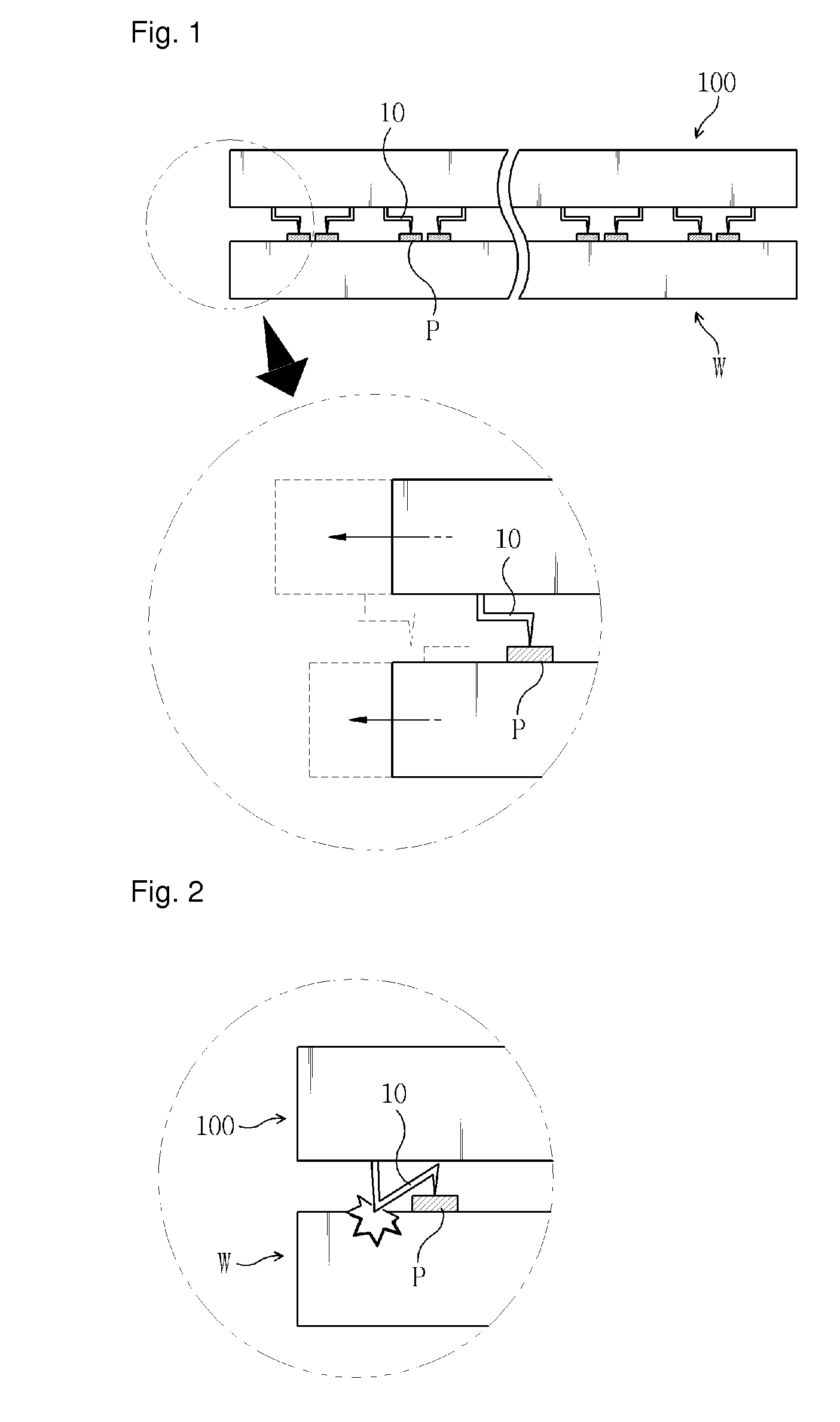
On the other hand, a conventional probe assembly has a problem of probe pin contact failure due to a difference in thermal expansion between the wafer and the probe assembly.
The probe pin contact failure often occurs while these tests are performed.
This problem may be more serious near edges of the probe assembly 100 as the size of the probe assembly 100 increases.
This problem is generated when equipment that adjusts the contact distance between the contact pad P of the wafer W and the probe pins 10 wrongly operates so that it moves by more than a contact tip height of the pins 10.
In this case, roots of the probe pins 10 as well as the surface of the wafer W may be remarkably damaged to cause a serious problem in the elasticity and position alignment of the probe pins 10.
In addition, the conventional probe assembly has various problems.
For example, problem assembly manufacturing time increases as the number of probe pins increases and electronic devices are required to be simply formed in the probe assembly together with the probe pins.

Method used


Image

  • Probe assembly and manufacturing method thereof
  • Probe assembly and manufacturing method thereof
  • Probe assembly and manufacturing method thereof

Examples


1st embodiment

Probe Assembly

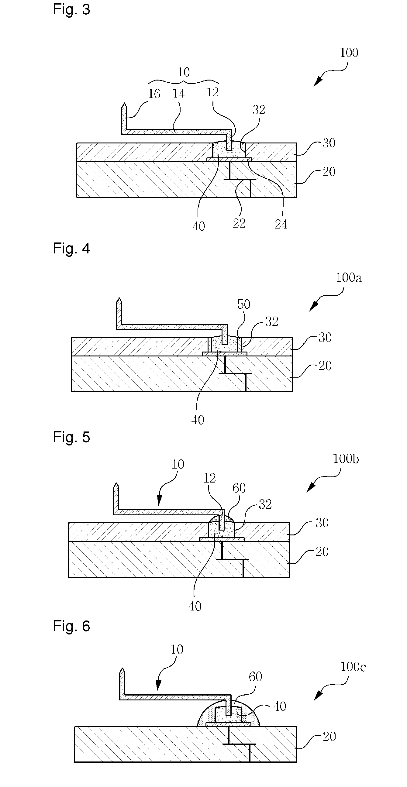
[0069]FIG. 3 is a cross-sectional view showing a probe assembly in accordance with a first embodiment of the present invention. Referring to FIG. 3, the probe assembly 100 is composed of probe pins 10, a circuit board 20, a base layer 30, and a conductive adhesive 40.

[0070]The circuit board 20, which is a printed circuit board (PCB) or a ceramic substrate, has a circuit pattern 22 formed therein and a plurality of pads 24 thereon. The circuit pattern 22, single-layered or multi-layered, is electrically connected to the pads 24 through via. The top surface of the circuit board 20 is covered with an insulating protective layer (not shown). The pads 24 are arranged with small pitch of several tens of micrometers throughout the top surface of the circuit board 20 without being covered with the protective layer. In general the circuit board 20 is combined with an interface board (not shown) of the probe card and electrically connected to a tester (not shown) through the int...

2nd embodiment

Probe Assembly

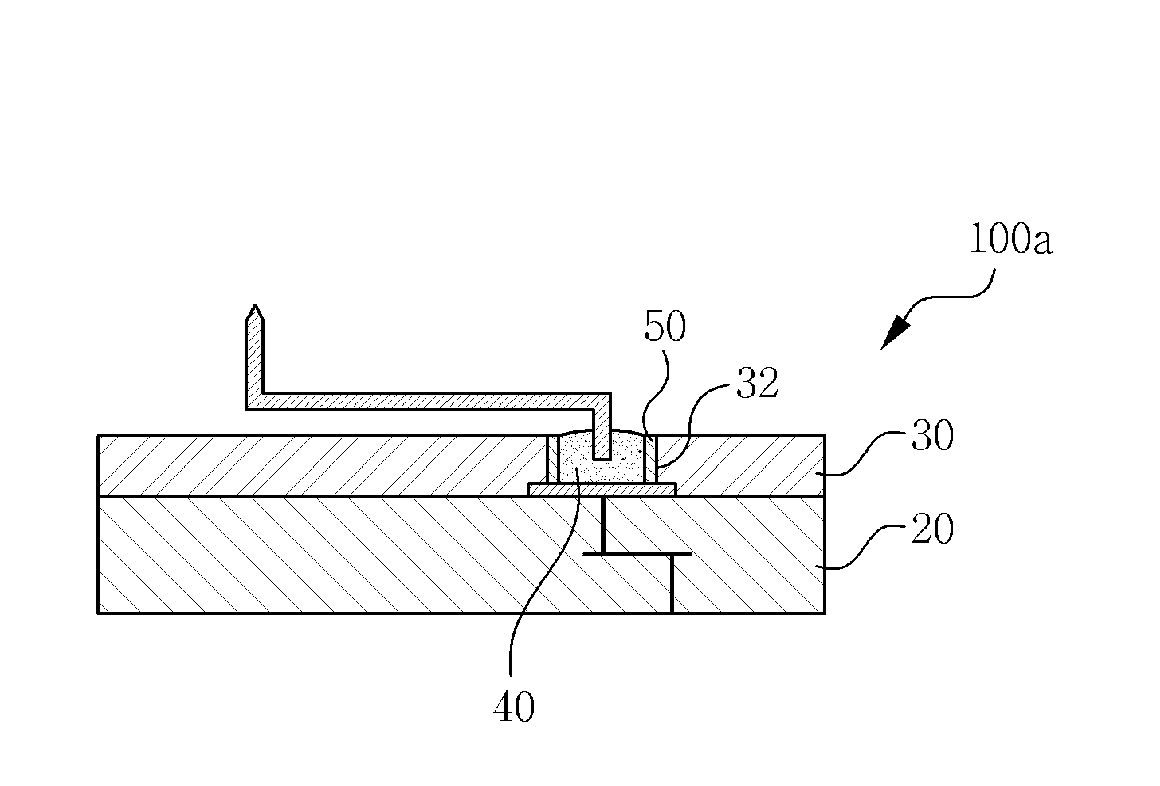
[0076]A probe assembly 100a shown in FIG. 4 is a case where a plating layer 50 is formed on sidewalls of the insertion hole 32 of the base layer 30.

[0077]The plating layer 50 in the insertion hole 32 may enhance the adhesive strength between the base layer 30 and the conductive adhesive 40. For that reason, the plating layer 50 may employ a material, such as gold, that has a good adhesive property with the conductive adhesive 40.

3rd embodiment

Probe Assembly

[0078]A probe assembly 100b shown in FIG. 5 is a case where a supporting agent 60 is used in addition to the conductive adhesive 40.

[0079]During a test, the probe pin 10 undergoes repeated mechanical contacts with the terminal of a target device. Therefore, due to fatigue stress, some of the probe pins 10 may deviate from an original position, fall down, or become deformed. In order to prevent such unfavorable results, the probe pins 10 should be firmly supported in the insertion holes 32 of the base layer 30. Of course, as discussed before, the conductive adhesive 40 that fully encloses the probe pin 10 in the insertion hole 32 can sufficiently support the probe pin 10. However, to maximize a supporting strength to the probe pin 10, the supporting agent 60 may be additionally used. The supporting agent 60 is formed on the conductive adhesive 40 and encloses the connectable root 12 of the probe pin 10, thus providing an additional supporting strength. Since the support...


PUM


Abstract

A probe assembly has insertion holes formed in a base layer provided on a circuit board. Probe pins are inserted into the insertion holes and fixed by a conductive adhesive filled in the insertion holes. The probe pins can be arranged with small pitch without mechanically electrically interfering with neighboring pins using the insertion holes. Furthermore, the base layer is formed of a semiconductor material to prevent a problem caused by a difference in the coefficient of thermal expansion between the base layer and a wafer. Moreover, coplanarity and alignment accuracy of the probe pins can be improved using aligning mask layers or aligning mask in a process of manufacturing the probe assembly. In addition, probe assembly manufacturing time can be reduced by using a pin array frame into which a large number of probe pins are temporarily inserted.

Description

TECHNICAL FIELD[0001]The present invention relates to a probe assembly and, more particularly, to a probe assembly of a probe card and a manufacturing method thereof.BACKGROUND ART[0002]In order to examine the electrical characteristics of small semiconductor devices (e.g., semiconductor chips in a wafer), a probe card is used as the medium of connection between a tester and a test target, i.e., semiconductor devices. As well known, such a semiconductor device has input / output terminals (also referred to as contact pads) exposed outwardly, and the probe card has probe pins that make a mechanical contact with the input / output terminals and also provide a path for electrical signals. That is, when receiving predetermined signals from the tester through the probe pins being in contact with the input / output terminals, the semiconductor device operates according to the received signals and then outputs the result to the tester through the probe pins.[0003]In general, for a rapid and effe...

Claims


Application Information

Patent Timeline
Patent Type & Authority Patents(United States)
IPC IPC(8): G01R31/00
CPCG01R1/06744G01R1/06727G01R3/00G01R1/07342
Inventor LEE, JAE HA
Owner LEE JAE HA
Learn More