
Delta-sigma modulator approach to increased amplifier gain resolution

a modulator and delta-sigma technology, applied in the field of variable gain amplifier circuits, can solve the problems of difficult to maintain high quantization precision over a wide-dynamic range, the unit size reduction impairs resistor matching on the integrated circuit, and the potential for large variation of audio input amplitude, etc., to achieve the effect of improving gain resolution and improving gain resolution

Inactive Publication Date: 2012-12-04
DIALOG SEMICONDUCTOR GMBH
View PDF26 Cites 12 Cited by
  • Summary
  • Abstract
  • Description
  • Claims
  • Application Information

AI Technical Summary

Benefits of technology

[0010]A further object of the present invention is to provide a variable gain input circuit device with improved gain resolution.
[0011]Another further object of the present invention is to provide a method to vary gain in an input circuit device.
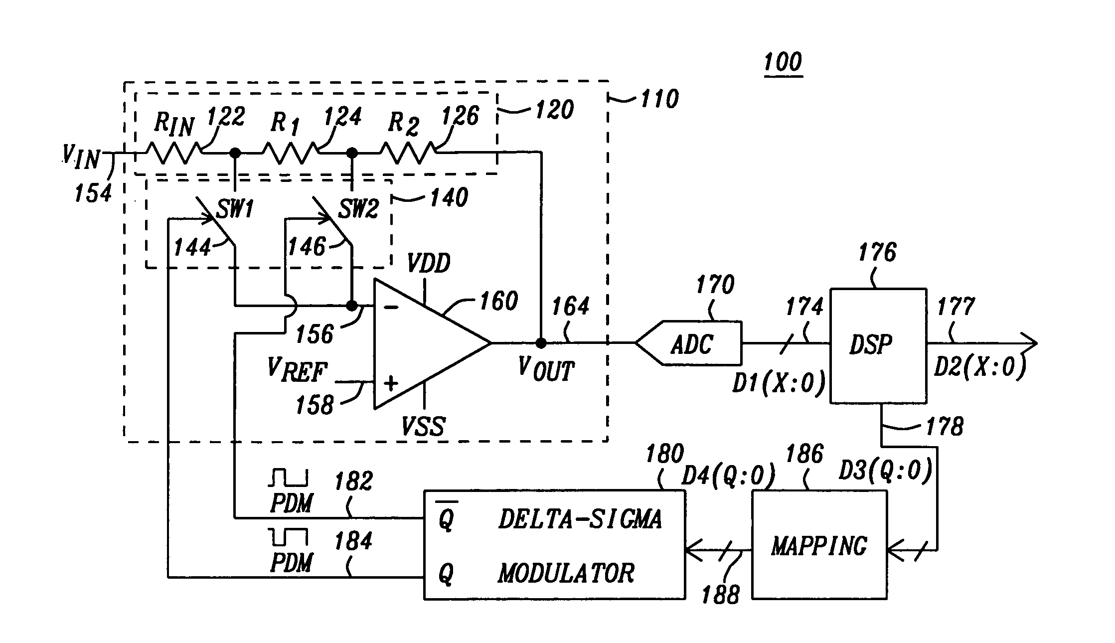
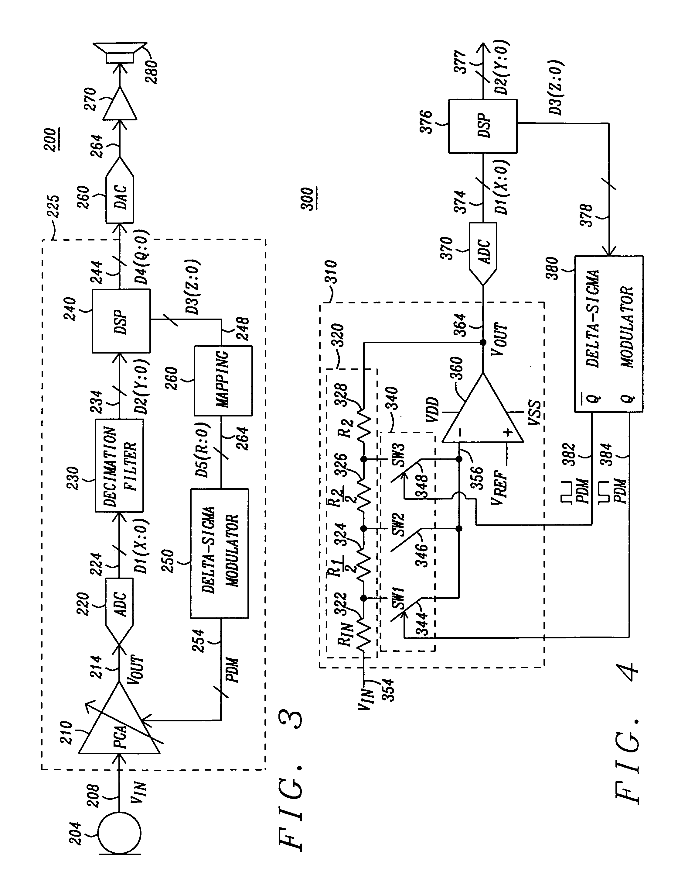
[0012]In accordance with the objects of this invention, a variable gain amplifier device with improved gain resolution is achieved. The device includes a programmable gain amplifier, an analog-to-digital converter, an automatic level control algorithm means, and a delta-sigma modulator. The programmable gain amplifier is capable to receive an analog input signal and to amplify the analog input signal to thereby generate an analog output signal. The programmable gain amplifier includes an amplifier and a switchable resistor network. The analog-to-digital converter is coupled to the programmable gain amplifier and is capable to convert the analog output signal to a digital signal. The automatic level control algorithm means is coupled to the analog-to-digital converter and is capable to generate a control code by processing the digital signal. The delta-sigma modulator is coupled to the automatic level control means and is capable to generate a pulse-density modulated signal by processing the control code. The pulse-density modulated signal is fed back to the programmable gain amplifier to control the switchable resistor network.
[0014]Also in accordance with the objects of this invention, a method to improve gain resolution in a programmable gain amplifier device is achieved. The method includes receiving an analog input signal at a programmable gain amplifier. The analog input signal is amplified to thereby generate an analog output signal. A gain of the programmable gain amplifier is adjusted by controlling a switchable resistor network. The analog output signal is converted to a digital signal. A control code is generated by processing the digital signal in an automatic level control (ALC) algorithm. A pulse-density modulated signal is generated by processing the control code in a delta-sigma modulator. The pulse-density modulated signal is fed back to the programmable gain amplifier to control the switchable resistor network.

Problems solved by technology

In portable electronic devices where external audio is captured and processed, an important issue is the potential for large variation of audio input amplitude as recording conditions change.
Large amplitude variation creates conflicting requirements for the ADC and makes it difficult to maintain high quantization precision over a wide-dynamic range.
This unit size reduction impairs resistor matching on the integrated circuit.
Conversely, if the proper unit size is maintained, then the additional series resistors will consume significant silicon area.
However, zero-cross detectors are undesirable for several reasons, including additional power and area requirements and significant circuit complexity.
Furthermore, zero-cross detectors are susceptible to problems caused by offset in the signal path or absence of a signal.
While noise gates can be used to alleviate these problems, noise gates limit the effective noise performance of the circuit.
However, gain changes that occur after digital quantization do not experience the same dynamic range improvement as found in the analog domain due to the fixed signal-to-noise ratio of the digital stages.
Further, the addition of the digital gain stages adds complexity to the ALC circuit, which must synchronize the gain changes to avoid audible distortion.
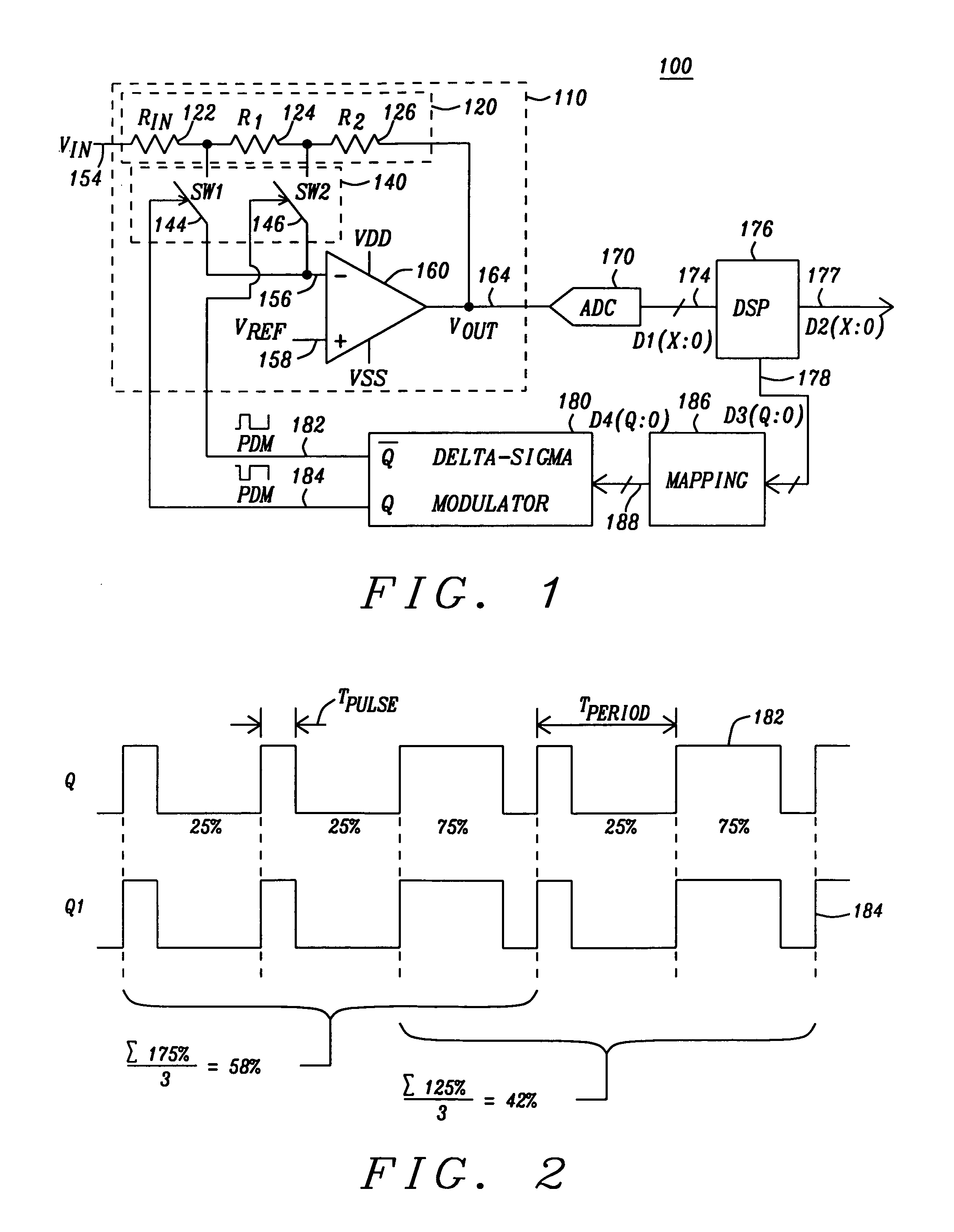
Integrated circuits are restricted in the maximum reference clock available due to power and circuit complexity constraints; thus limiting the gain-resolution practically achievable using only PWM.

Method used


Image

  • Delta-sigma modulator approach to increased amplifier gain resolution
  • Delta-sigma modulator approach to increased amplifier gain resolution
  • Delta-sigma modulator approach to increased amplifier gain resolution

Examples


Embodiment Construction

[0024]FIG. 1 is a circuit schematic diagram illustrating one example of a variable gain amplifier device 100 in accordance with one embodiment of the invention. The device 100 includes a programmable gain amplifier (PGA) 110, an analog-to-digital converter 170, and a delta-sigma modulator 180. The programmable gain amplifier 110 includes an amplifier 160 having an input 156 and an output 164, and a switchable resistor network 120. The switchable resistor network 120 includes resistors 122, 124, and 126, and switches 144 and 146. The resistor RIN 122, R1 124, and R2 126 are arranged in series from the PGA input VIN 154 to the PGA output VOUT 164. The switches SW1144 and SW2146 arranged between the amplifier input 156 and nodes between the resistors 122, 124, and 126. The amplifier 160 is preferably an operational amplifier with inverting and non-inverting inputs as is known in the art. While a single-ended amplifier is shown, a differential input / output amplifier may alternatively be...


PUM


Abstract

A variable gain amplifier device (100) with improved gain resolution is achieved. The device includes a programmable gain amplifier (PGA) (110), an analog-to-digital converter (ADC) (160), an automatic level control (ALC) algorithm means (176), and a delta-sigma modulator (180). The PGA (110) is capable to receive and to amplify an analog input signal (154) to thereby generate an analog output signal (164). The PGA (110) includes an amplifier (160) and a switchable resistor network (120). The ADC (170) is coupled to the PGA (110) and is capable to convert the analog output signal (164) to a digital signal (174). The ALC algorithm means (176) is coupled to the ADC (170) and is capable to generate a control code (178) by processing the digital signal (174). The delta-sigma modulator (186) is coupled to the ALC algorithm means (186) and is capable to generate a pulse-density modulated (PDM) signal (182) by processing the control code (178). The PDM signal (182) is fed back to the PGA (110) to control the switchable resistor network (120).

Description

FIELD OF THE INVENTION[0001]The invention relates generally to variable gain amplifier circuits and methods and, more particularly, to a variable gain amplifier circuit device having improved gain resolution and a method thereof.BACKGROUND OF THE INVENTION[0002]Digital Signal Processors (DSP) are frequently incorporated into modern integrated circuits due to the flexibility and reliability provided in these processing circuits. DSP circuits are used to implement complex audio functions such as echo cancellation, audio equalization effects, and encoding. In some applications, it is desirable to digitally process an analog signal using the DSP. For example, it may be desirable to capture, process, and reproduce an external audio source, such as a human voice or music. This audio signal must first be captured as an analog signal, typically using a microphone, and then converted to a digital format prior to processing in the DSP circuit. An analog-to-digital converter (ADC) is typically...

Claims


Application Information

Patent Timeline
Patent Type & Authority Patents(United States)
IPC IPC(8): H03G3/12
CPCH03G1/0088H03G3/001H03G3/3026
Inventor LOEDA, SEBASTIANMUIR, ALISDAIR
Owner DIALOG SEMICONDUCTOR GMBH
Learn More