Improving back-contact performance of group VI containing solar cells by utilizing a nanoscale interfacial layer

a solar cell and nano-scale technology, applied in the field of photovoltaic devices containing a group vi element, can solve the problems of requiring a significant requiring a large amount of raw materials, and being relatively less efficient and less expensive, so as to increase the efficiency and service life of a photovoltaic device.

Inactive Publication Date: 2012-11-13
FOREHAND DAVID
View PDF13 Cites 16 Cited by
  • Summary
  • Abstract
  • Description
  • Claims
  • Application Information

AI Technical Summary

Benefits of technology

[0014]The present invention is a method of making a diffusion-impeding barrier layer, also known as interfacial layer (IFL), within a photovoltaic cell comprising, for example, cadmium telluride, cadmium sulfide, and a metal-comprising electrical contact, by exposing the surface of the cadmium telluride layer to a halogen (e.g., fluorine) to create a Te-poor cadmium fluoride barrier layer. The present invention is not limited to copper and will work for any metal electrical contact metal, as well as any material comprising any a Group II-VI element, including but not limited to CuInGaSe photovoltaic material, also known as CIGS. Although specific reference is made to CdTe photovoltaics, the invention is not limited thereto. A skilled artisan will appreciate that virtually any photovoltaic material can benefit from the teachings herein. By inhibiting metal diffusion and maintaining the integrity of the electrical contact, these compounds increase the efficiency and serviceable lifetime of a photovoltaic.
[0015]For example, the present invention provides a more thermally stable, low-resistance contact on a p-type CdTe photovoltaic cell by forming a Te-poor barrier layer of CdF2, which is a more thermodynamically stable compound than CdTe, Cu2Te, or CuTe, by exposing the p-type layer to a fluorine-containing plasma. The CdF2 compound inhibits the diffusion of copper, or other contact metal. By inhibiting Cu-diffusion, the efficiency of the CdTe photovoltaic cell and the serviceable lifetime are increased.
[0016]Surprisingly, and contrary to standard industry practice of creating Te-rich surfaces on CdTe layers, it has been found that creating a Te-poor surface provides a diffusion-inhibiting barrier layer that impedes the diffusion of metal from, for example, a metal contact. The formation of a, for example, cadmium fluoride layer provides several unique features including but not limited to: providing a barrier between CdTe, or other Group II-VI containing compounds and the contact to significantly reduce the diffusion of Cu or other contact metals; creating a Te-poor surface; creating a more uniform type II-VI surfaces (e.g., p-CdTe surface), by reducing the effects of weak-diodes and increasing PV performance uniformity across the PV module and module-to-module; cleaning the CdTe surface or other II-VI compound surfaces; ability to passivate CdTe, or other II-VI compounds and grain boundaries; and ability to adjust or tailor the thickness depending on the II-VI compound and metal contact material. The technique is a dry process and requires a relatively short amount of processing time, thereby allowing easy process flow integration. In addition, a thinner absorber layer may be used. For example, a p-CdTe layer of less than about 2 microns thick may be used instead of the current industry standard 4-10 microns. This would have the added advantages of lower material utilization, faster throughput, and greater charge collection due to the lower recombination.
[0017]For a copper-containing contact metal on p-CdTe, the cadmium fluoride barrier layer should be of a thickness that impedes the diffusion of copper through the cell while allowing tunneling current from the p-type cadmium telluride layer to the back contact. In one embodiment, the thickness is less than about 25 nm or less than about 10 nm. The CdF2 barrier layer facilitates the establishment of a thermally-stable low-resistance contact between the p-type cadmium telluride layer and the back contact, which increases the efficiency and lifetime of the photovoltaic cell.
[0019]In some embodiments, the forming step may create a copper fluoride barrier layer between the diffusion impedance barrier layer and the electrical contact. In some embodiments, the diffusion impedance barrier layer impedes the diffusion of a metal from the electrical contact into the p-type layer. In other embodiments, the impedance barrier layer may have a thickness of about 0.5 to about 25 nanometers. In some embodiments, the impedance barrier layer allows the tunneling of current from the p-type layer of the photovoltaic cell to the electrical contact. Some embodiments may include the step of creating a second diffusion impedance barrier layer atop the p-type layer by exposing at least one surface of the first diffusion impedance barrier layer to a halogen (e.g., fluorine).

Problems solved by technology

Single crystal photovoltaic cells exhibit high operation performance, up to 25-30% conversion efficiency, but are relatively costly to manufacture, and require a significant amount of raw materials.
Polycrystalline and amorphous materials can also be used however they are relatively less efficient and less expensive.
However, a stable, low-resistance ohmic contact with p-CdTe is very difficult to obtain due to CdTe's band gap and high electron affinity.
Unfortunately, no metal satisfies this requirement.
Thus, the Schottky barrier diode blocks the desired flow of photo-generated charge carriers, greatly increasing the resistance of the back contact and limiting the total cell current generated, which ultimately reduces the efficiency of the solar cell.
Copper has another more dubious distinction; its diffusion is known to be one of the main causes of instability and degradation of the performance CdTe photovoltaic cells.
This Cu diffusion causes the back contact to degrade, making the contact more resistive, less able to transport charge carriers, and its accumulation decreases cell performance and stability.
Although copper can react with tellurium to form Cu2Te, thought to be a beneficial compound, it is believed that this compound is less thermodynamically favorable than CdTe.
However, there currently is no definitive solution that provides an efficient method to create a stable low-resistance back contact in CdTe photovoltaic cells.

Method used


Image

  • Improving back-contact performance of group VI containing solar cells by utilizing a nanoscale interfacial layer
  • Improving back-contact performance of group VI containing solar cells by utilizing a nanoscale interfacial layer

Examples


Embodiment Construction

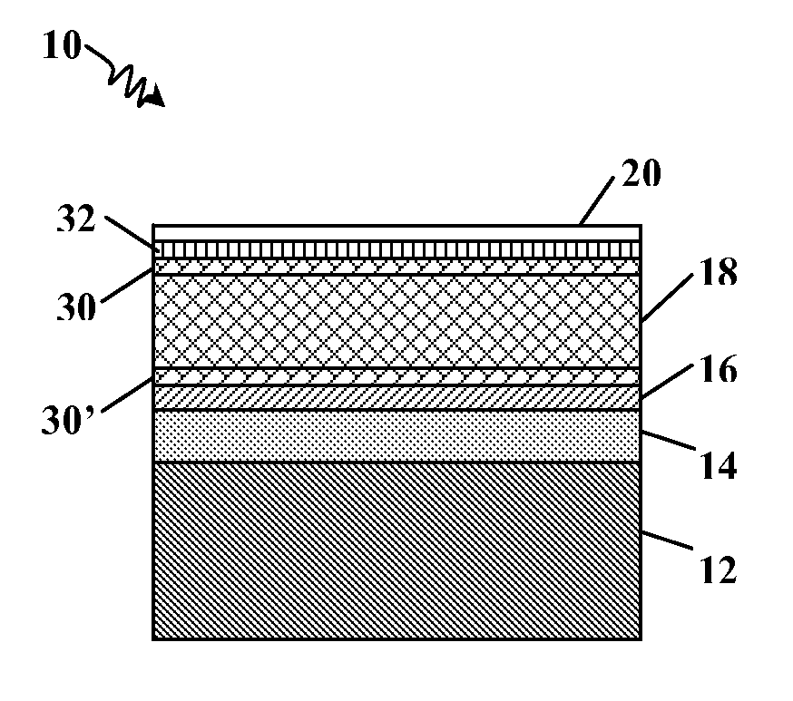
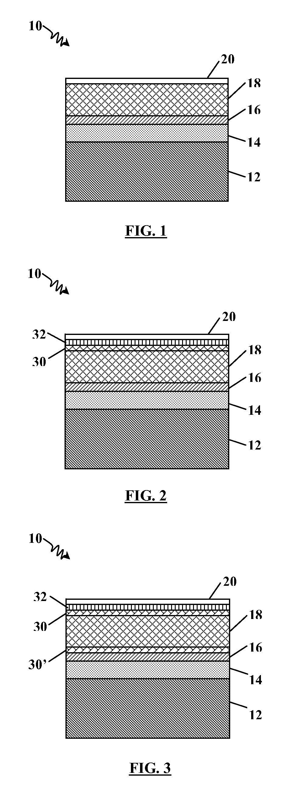
[0030]In the following detailed description, reference may be made to the drawings, which show by way of illustration specific embodiments in which the invention may be practiced. These embodiments are described in sufficient detail to enable those skilled in the art to practice the invention, and it will be understood by the skilled artisan that other embodiments may be utilized. It is also to be understood that structural, procedural and system changes may be made without departing from the spirit and scope of the present invention. The following detailed description, therefore, is not to be taken in a limiting sense, and the scope of the present invention is defined by the appended claims and their equivalents. For clarity of exposition, like features shown in the accompanying drawings are indicated with like reference numerals and similar features as shown in alternate embodiments in the drawings are indicated with similar reference numerals. FIGS. 1 and 2 are enlarged cross-sec...


PUM


Abstract

A method of making thermodynamically stable, diffusion-impeded barrier layers within, for example, a photovoltaic cell with a metal-containing electrical contact using exposure to fluorine. Exposing the cadmium telluride surface to fluorine creates a Te-poor barrier layer of cadmium fluoride. Once that barrier layer is formed, the metal-containing electrical contact may be applied or formed. The barrier layer allows tunneling current to occur between the p-type layer and the metal-containing electrical contact establishing a low-resistance, highly uniform, and thermally stable electrical contact.

Description

CROSS REFERENCE TO RELATED APPLICATIONS[0001]This application claims the benefit of U.S. provisional patent application No. 60 / 911,543, filed Apr. 13, 2007, which is incorporated herein by reference.BACKGROUND OF THE INVENTION[0002]1. Technical Field[0003]The present invention relates generally to photovoltaic devices containing a Group VI element. More particularly, this invention relates to the creation of thermodynamically stable, non-moving compounds within a photovoltaic device, for example having a cadmium telluride p-type layer with a metal-containing (e.g., copper-containing) electrical contact, upon exposure to fluorine atoms (e.g., via plasma treatment).[0004]2. Description of Related Art[0005]The need for affordable, renewable sources of energy has become more of a focus of public interest and scientific research in light of the rising price of traditional energy sources. Photovoltaic cells have the ability to convert sunlight, a practically infinite energy source, into d...

Claims


Application Information

Patent Timeline
Patent Type & Authority Patents(United States)
IPC IPC(8): H01L21/00H01L31/00
CPCH01L31/073H01L31/1828Y02E10/543Y02P70/50
Inventor FOREHAND, DAVID
Owner FOREHAND DAVID
Why Eureka
Try Eureka