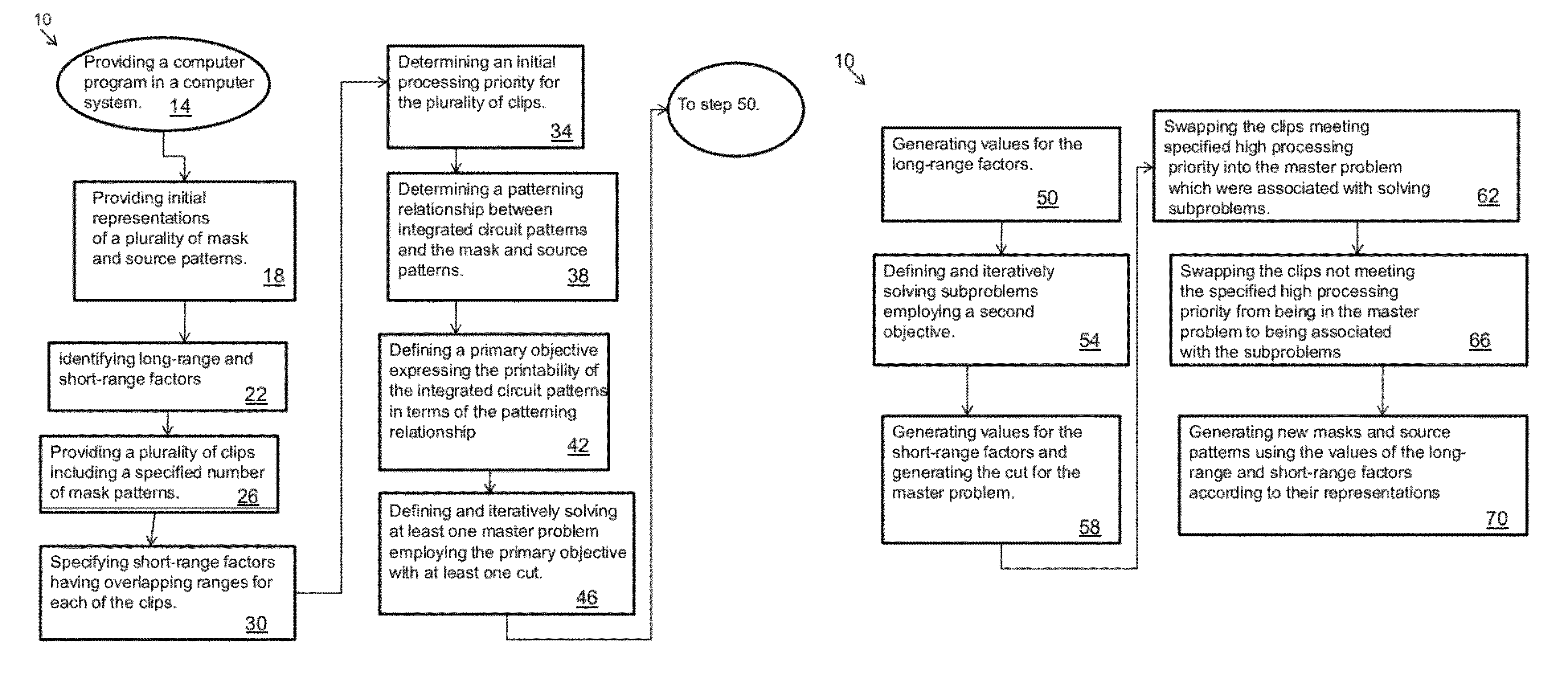
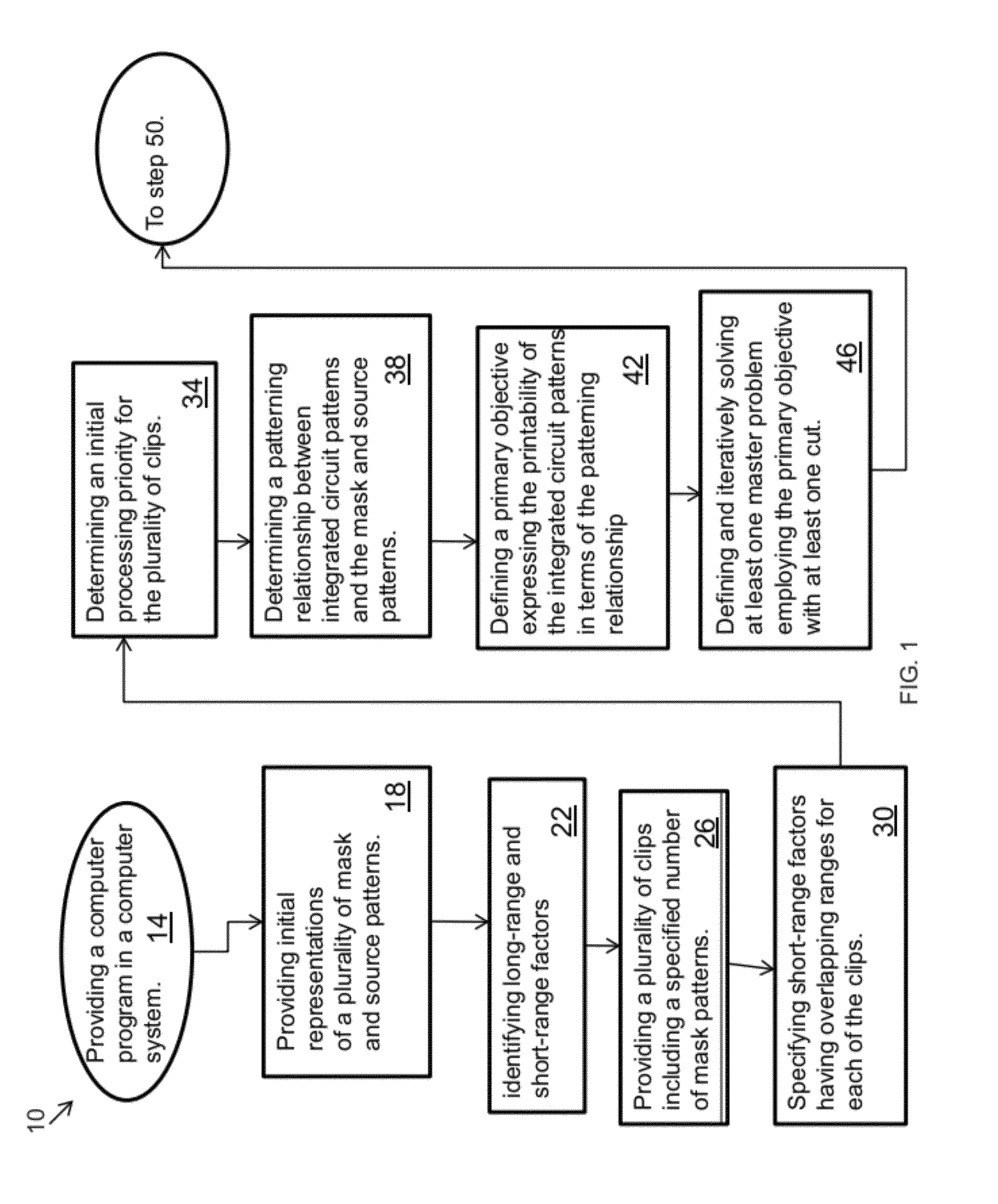
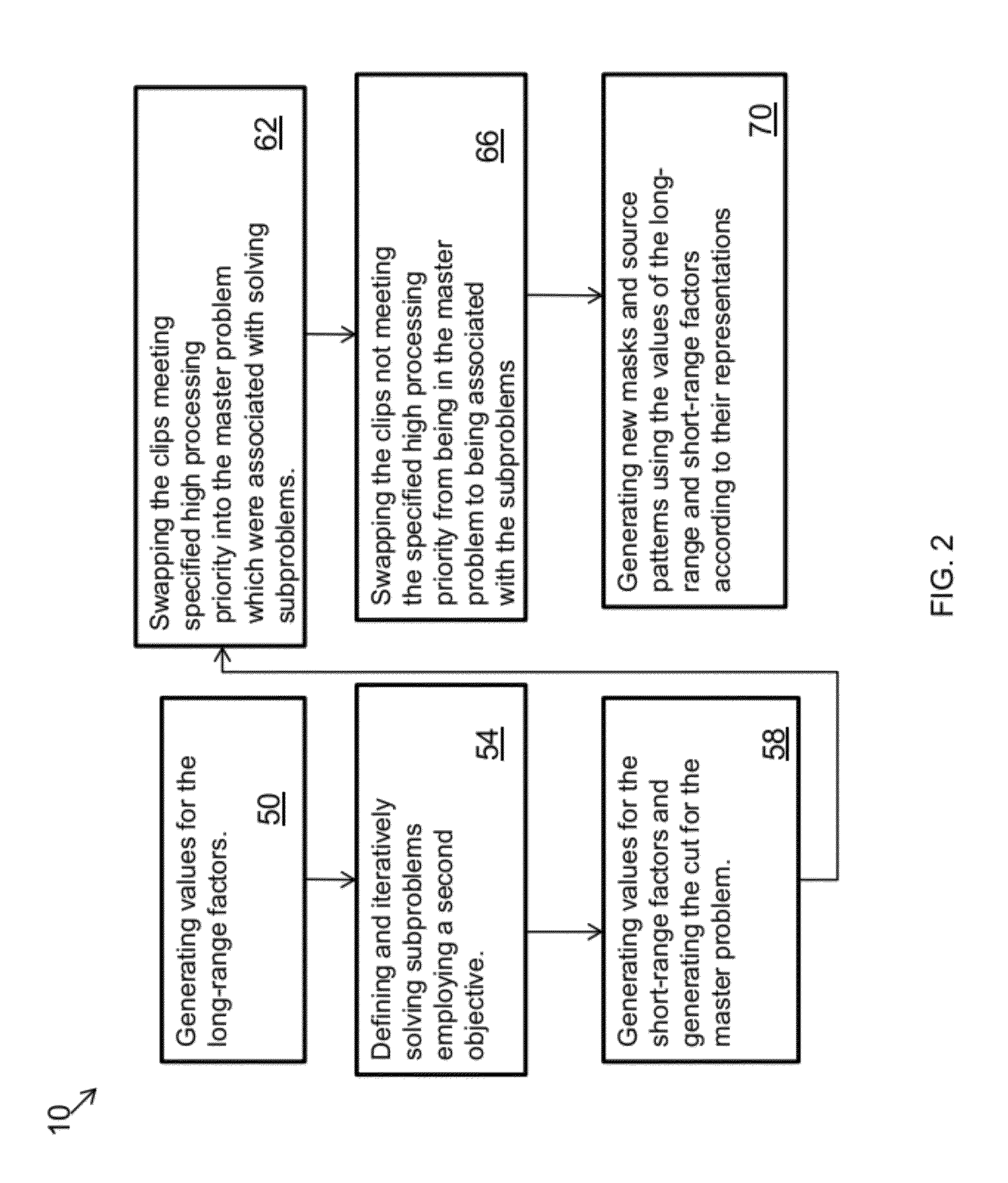
Dynamic provisional decomposition of lithographic patterns having different interaction ranges
a technology of dynamic provisional decomposition and lithographic pattern, which is applied in the field of semiconductor manufacturing photolithography, can solve the problems of increasing costs, reducing the number of exposure tools used to form circuit patterns, and approaching technological limits, so as to achieve the effect of increasing the density of the circuit, and increasing the cos
- Summary
- Abstract
- Description
- Claims
- Application Information
AI Technical Summary
Benefits of technology
Problems solved by technology
Method used
Image

Examples
example problem
[0100]
minzs.t.0≤x≤10≤z≤62x+y12≤zx+2y1≥40≤y1≤104x+2y22≤z3x+y2≥20≤y2≤10Simple idea:Alternatingly fix subset of variables:Fix x (sources) and optimize (z, yi)In SMO: Mask-Only OptimizationFix yi (masks) and optimize (x, z)In SMO: Source-Only OptimizationFor this example:Start with x = 0Gives yl = 2, z = 4 and y2 = 2, z = 8Fix yl = 2, y2 = 2Cannot increase x without makingobjective function worseThis procedure stops with x = 0, z = 8suboptimal, even though this problem isconvex (= simple)
[0101]Benders Decomposition: Master Problem
[0102]
minx,yigTxs.t.Ax=bxL≤x≤xUBi(x,yi)=0yLi≤yi≤yiU(Linear) Master problem (MP):minxgTxs.t.Ax=bcjTx≤djxL≤x≤xU(MP)Only in small x spaceOverestimates set of feasible xIdea: Iteratively add “cuts” cTjx ≦ djto approximate F increasingly tighterOnce cuts are very tight on F, solutionof (MP) is solution for original problem
[0103]Benders Decomposition: Cut Generation
[0104]
In each iteration: Solve (MP) to get xCheck if x is feasible for constraints ...
PUM
 Abstract
Description
Claims
Application Information
 - R&D
- Intellectual Property
- Life Sciences
- Materials
- Tech Scout
- Unparalleled Data Quality
- Higher Quality Content
- 60% Fewer Hallucinations
Browse by: Latest US Patents, China's latest patents, Technical Efficacy Thesaurus, Application Domain, Technology Topic, Popular Technical Reports.
© 2025 PatSnap. All rights reserved.Legal|Privacy policy|Modern Slavery Act Transparency Statement|Sitemap|About US| Contact US: help@patsnap.com