
Dicing tape-integrated wafer back surface protective film

a protective film and tape-integrated technology, applied in the direction of layered products, transportation and packaging, chemistry apparatus and processes, etc., can solve the problems of increasing the number of steps, increasing the cost and the like, and the damage of semiconductor chips, and achieve excellent holding force

Inactive Publication Date: 2012-08-07
NITTO DENKO CORP
View PDF16 Cites 4 Cited by
  • Summary
  • Abstract
  • Description
  • Claims
  • Application Information

AI Technical Summary

Benefits of technology

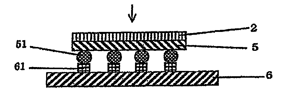
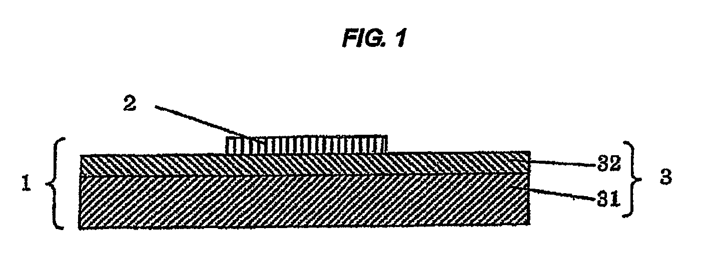
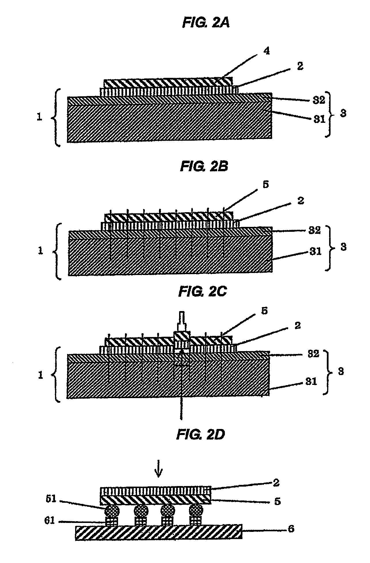
The present invention provides a solution for attaching a protective film to a semiconductor chip during the dicing and picking-up steps. By using a dicing tape with a pressure-sensitive adhesive layer and a colored wafer back surface protective film, the protective film can be attached to the chip during the dicing step and can exhibit excellent holding force and marking properties after the picking-up step. This eliminates the need for a separate step of attaching the protective film and improves the efficiency of the process. The invention also provides a method for producing a semiconductor device using this protective film and a flip chip-mounted semiconductor device that includes the protective film attached to the chip.

Problems solved by technology

However, the attachment of a back surface protective film for protecting a back surface of a semiconductor chip to the back surface of the semiconductor chip obtained by dicing a semiconductor wafer in a dicing step results in the addition of a step for the attachment, so that the number of steps increases and cost and the like increase.
Moreover, owing to the thinning, the semiconductor chip may be damaged in some cases in a picking-up step of the semiconductor chip after the dicing step.

Method used


Image

  • Dicing tape-integrated wafer back surface protective film
  • Dicing tape-integrated wafer back surface protective film
  • Dicing tape-integrated wafer back surface protective film

Examples


example 1

Manufacture of Colored Wafer Back Surface Protective Film

[0142]113 parts of an epoxy resin (trade name “EPICOAT 1004” manufactured by JER Co., Ltd.), 121 parts of a phenol resin (trade name “MILEX XLC-4L” manufactured by Mitsui Chemicals, Inc.), 246 parts of sphere silica (trade name “SO-25R” manufactured by Admatechs Co., Ltd., average particle diameter: 0.5 μm), 5 parts of a dye 1 (trade name “OIL GREEN 502” manufactured by Orient Chemical Industries Co., Ltd.), and 5 parts of a dye 2 (trade name “OIL BLACK BS” manufactured by Orient Chemical Industries Co., Ltd.) based on 100 parts of an acrylic acid ester-based polymer (trade name “PARACRON W-197CM” manufactured by Negami Chemical Industrial Co., Ltd.) having ethyl acrylate and methyl methacrylate as main components were dissolved into methyl ethyl ketone to prepare a resin composition solution having a solid concentration of 23.6% by weight.

[0143]The resin composition solution was applied onto a releasably treated film as a rel...

example 2

Manufacture of Colored Wafer Back Surface Protective Film

[0145]113 parts of an epoxy resin (trade name “EPICOAT 1004” manufactured by JER Co., Ltd.), 121 parts of a phenol resin (trade name “MILEX XLC-4L” manufactured by Mitsui Chemicals, Inc.), 246 parts of sphere silica (trade name “SO-25R” manufactured by Admatechs Co., Ltd., average particle diameter: 0.5 μm), 10 parts of a dye 1 (trade name “OIL GREEN 502” manufactured by Orient Chemical Industries Co., Ltd.), and 10 parts of a dye 2 (trade name “OIL BLACK BS” manufactured by Orient Chemical Industries Co., Ltd.) based on 100 parts of an acrylic acid ester-based polymer (trade name “PARACRON W-197CM” manufactured by Negami Chemical Industrial Co., Ltd.) having ethyl acrylate and methyl methacrylate as main components were dissolved into methyl ethyl ketone to prepare a resin composition solution having a solid concentration of 23.6% by weight.

[0146]The resin composition solution was applied onto a releasably treated film as a r...

example 3

Manufacture of Colored Wafer Back Surface Protective Film

[0148]32 parts of an epoxy resin (trade name “EPICOAT 1004” manufactured by JER Co., Ltd.), 35 parts of a phenol resin (trade name “MILEX XLC-4L” manufactured by Mitsui Chemicals, Inc.), 90 parts of sphere silica (trade name “SO-25R” manufactured by Admatechs Co., Ltd., average particle diameter: 0.5 μm), 3 parts of a dye 1 (trade name “OIL GREEN 502” manufactured by Orient Chemical Industries Co., Ltd.), and 3 parts of a dye 2 (trade name “OIL BLACK BS” manufactured by Orient Chemical Industries Co., Ltd.) based on 100 parts of an acrylic acid ester-based polymer (trade name “PARACRON W-197CM” manufactured by Negami Chemical Industrial Co., Ltd.) having ethyl acrylate and methyl methacrylate as main components were dissolved into methyl ethyl ketone to prepare a resin composition solution having a solid concentration of 23.6% by weight.

[0149]The resin composition solution was applied onto a release-treated film as a releasabl...


PUM

PropertyMeasurementUnit
thicknessaaaaaaaaaa
particle diameteraaaaaaaaaa
thicknessaaaaaaaaaa

Abstract

The present invention provides a dicing tape-integrated wafer back surface protective film including: a dicing tape including a base material and a pressure-sensitive adhesive layer formed on the base material; and a wafer back surface protective film formed on the pressure-sensitive adhesive layer of the dicing tape, in which the wafer back surface protective film is colored. It is preferable that the colored wafer back surface protective film has a laser marking ability. The dicing tape-integrated wafer back surface protective film can be suitably used for a flip chip-mounted semiconductor device.

Description

FIELD OF THE INVENTION[0001]The present invention relates to a dicing tape-integrated wafer back surface protective film. A dicing tape-integrated wafer back surface protective film is used for protecting a back surface of a chip-shaped workpiece (such as a semiconductor chip) and enhancing strength. Moreover, the invention relates to a semiconductor device using the dicing tape-integrated wafer back surface protective film and a process for producing the device.BACKGROUND OF THE INVENTION[0002]Recently, thinning and miniaturization of a semiconductor device and its package have been increasingly demanded. Therefore, as the semiconductor device and its package, those in which a semiconductor chip (chip-shaped workpiece) is fixed to a substrate in a form where a circuit face of the semiconductor chip is opposed to an electrode-formed face of the substrate (one produced by flip chip bonding; it may be referred as a flip chip-mounted semiconductor device) have been widely utilized. In ...

Claims


Application Information

Patent Timeline
Patent Type & Authority Patents(United States)
IPC IPC(8): H01L23/48H01L23/52H01L29/40
CPCH01L23/562H01L23/544H01L21/6836H01L24/81H01L2924/0102H01L2221/68327H01L2924/01025H01L2924/01004Y10T428/2848H01L2224/81801Y10T428/1467H01L2924/01079H01L2224/16H01L2223/5448H01L2924/01019Y10T428/28H01L2224/27436H01L2924/01046H01L2924/00011H01L2924/00014H01L2924/12042Y10T428/31511H01L2924/00H01L2224/0401
Inventor TAKAMOTO, NAOHIDEMATSUMURA, TAKESHI
Owner NITTO DENKO CORP
Learn More