
Semi-polar semiconductor light emission devices

a semiconductor and light-emitting device technology, applied in the direction of semiconductor devices, basic electric elements, electrical equipment, etc., can solve the problems of high cost of solid-state light-emitting devices, complex manufacturing process, high defect density, etc., and achieve low defect density and improve device reliability and lifetime.

Active Publication Date: 2012-07-10
SIPHOTON
View PDF47 Cites 29 Cited by
  • Summary
  • Abstract
  • Description
  • Claims
  • Application Information

AI Technical Summary

Benefits of technology

[0008]The disclosed devices may have certain advantages, including that they can provide single GaN crystals with very low defect density, which improves device reliability and lifetime; they can be tailored in different form factors to suit different applications; and they can be fabricated on a silicon substrate, which is compatible with many microelectronic devices.

Problems solved by technology

Although solid-state lighting offers certain advantages, conventional semiconductor structures and devices used for solid-state lighting are relatively expensive.
The high cost of solid-state light emitting devices is partially related to their relatively complex and time-consuming manufacturing process.
Although it was found that the light emission of these LED structures were spectrally stable and polarized, the emission intensities were low due to numerous defects formed in the GaN crystals during growth on the LiAlO2 substrate.

Method used


Image

  • Semi-polar semiconductor light emission devices
  • Semi-polar semiconductor light emission devices
  • Semi-polar semiconductor light emission devices

Examples


Embodiment Construction

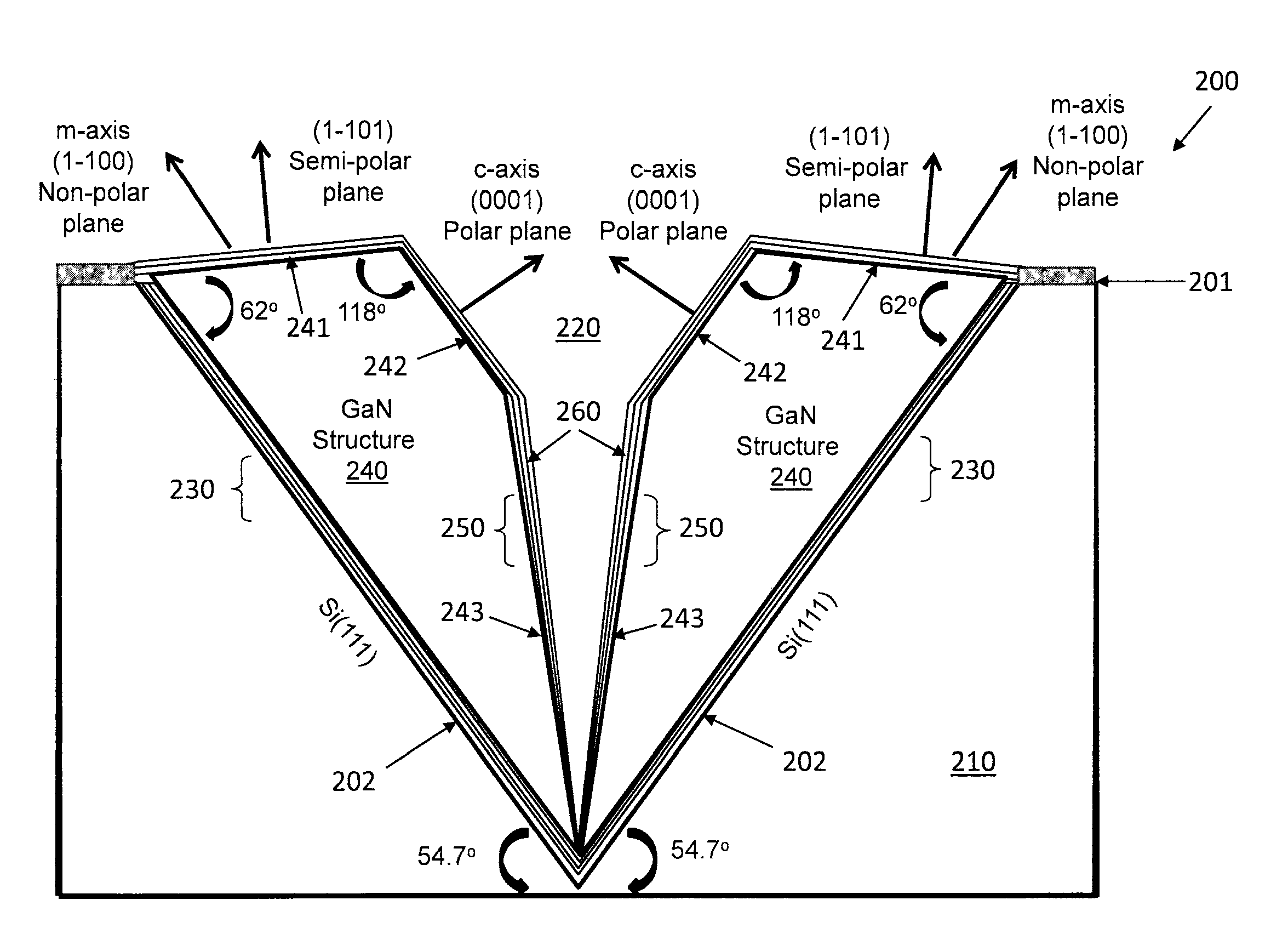
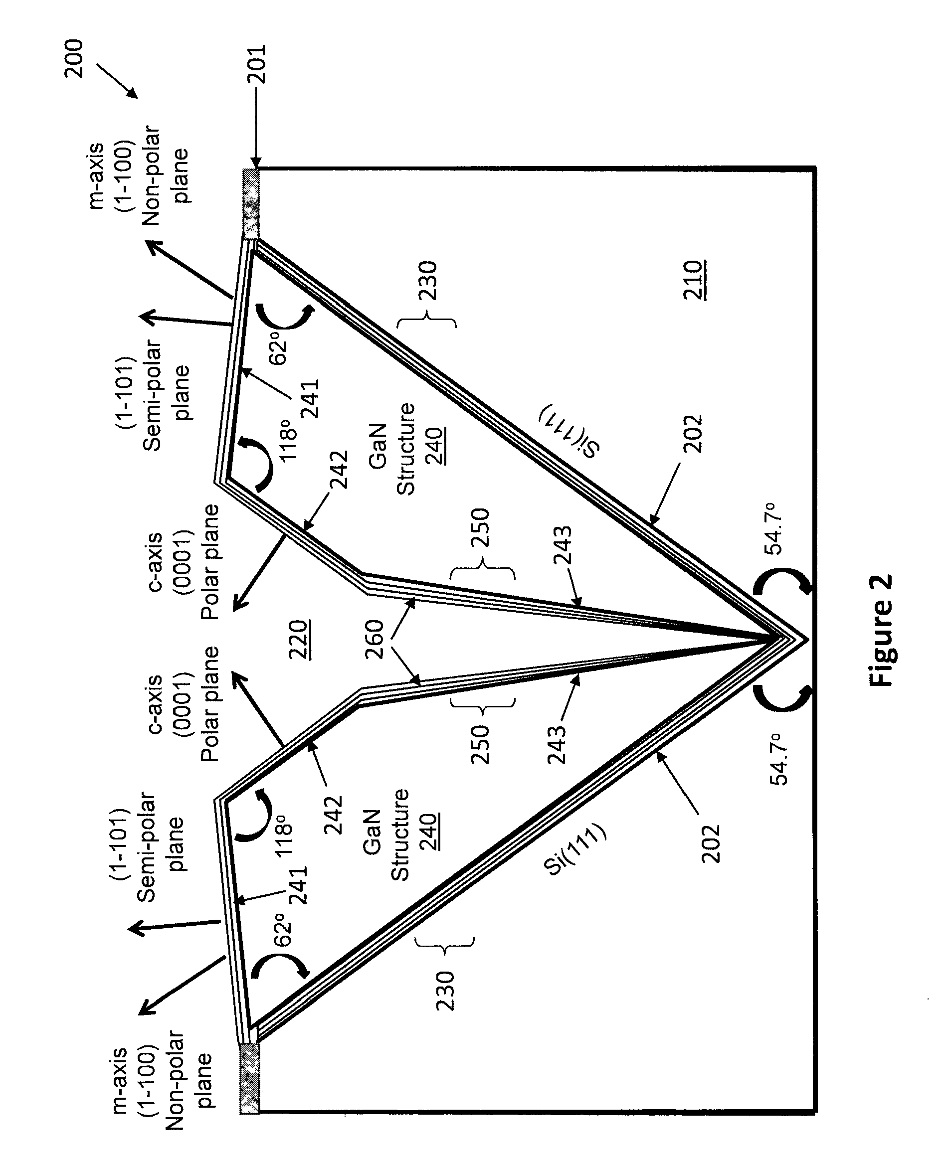
[0026]Referring to FIG. 2, a light emitting device 200 includes a silicon substrate 210 having a (100) upper surface 201, a recess 220 defined at least in part by (111) surfaces 202, buffer and reflective layers 230 on the surfaces 202, a doped GaN crystal structure 240 on the buffer and reflective layers 230, light emission layers comprising quantum well layers 250 on the doped GaN crystal structure 240, and a doped GaN layer 260 on the quantum well layers 250. The doped GaN crystal structure 240 and the doped GaN layer 260 are conductive and can respectively serve as lower and upper electrodes for the quantum well layers 250.

[0027]A recess 220 in the light emitting device 200 is formed in the (100) upper surface 201 of the silicon substrate 210. A SiN mask (not shown) formed on the (100) upper surface can have square or rectangle openings. The dimensions of each side of these openings can be in the range from tens of microns to a few millimeters. Etching through openings in the Si...


PUM


Abstract

A light emitting device includes a silicon substrate comprising a (111) surface and a GaN crystal structure over the (111) surface of the silicon substrate. The GaN crystal structure includes a first surface along a semi-polar plane of the GaN crystal structure and a second surface along a polar plane of the GaN crystal structure. The light emitting device also includes light emission layers over the first surface of the GaN crystal structure. The light emission layers include at least one quantum well comprising GaN.

Description

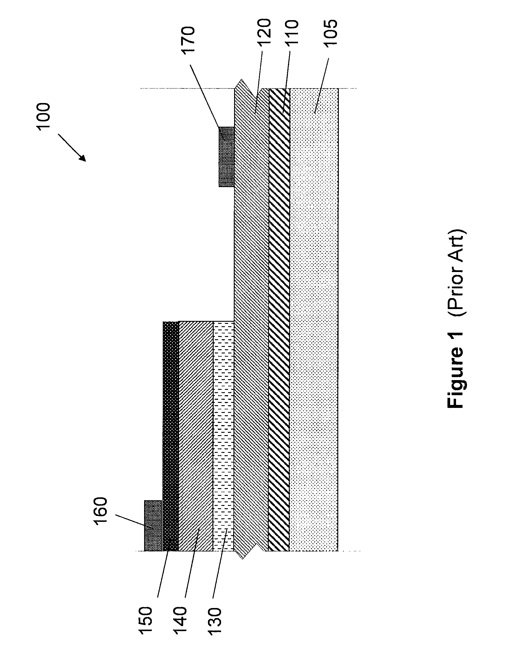
BACKGROUND OF THE INVENTION[0001]This patent application is related to solid state light emitting devices.[0002]Solid-state light sources, such as light emitting diodes (LEDs) and laser diodes, can offer significant advantages over incandescent or fluorescent lighting. Solid-state light sources are generally more efficient and produce less heat than traditional incandescent or fluorescent lights. When LEDs or laser diodes are placed in arrays of red, green and blue elements, they can act as a source for white light or as a multi-colored display. Although solid-state lighting offers certain advantages, conventional semiconductor structures and devices used for solid-state lighting are relatively expensive. The high cost of solid-state light emitting devices is partially related to their relatively complex and time-consuming manufacturing process.[0003]Referring to FIG. 1, a prior art LED structure 100 includes a substrate 105, such as sapphire. A buffer layer 110 is formed on the sub...

Claims


Application Information

Patent Timeline
IPC IPC(8): H01L33/00
CPCH01L33/18H01L33/32H01L33/20
Inventor PAN, SHAOHER X.CHEN, JAYPAYNE, JUSTINHEUKEN, MICHAEL
Owner SIPHOTON
Learn More