
Strained transistor and method for forming the same

a transistor and straining technology, applied in the direction of transistors, semiconductor devices, electrical equipment, etc., can solve the problems of difficult to precisely apply the strain to the channel region, difficult process steps, and many additional masks, and achieve the effect of preventing parasitic effects

Active Publication Date: 2012-07-10
STMICROELECTRONICS SRL
View PDF24 Cites 7 Cited by
  • Summary
  • Abstract
  • Description
  • Claims
  • Application Information

AI Technical Summary

Benefits of technology

The solution effectively increases carrier mobility, enhances transistor performance, and minimizes defects by directly applying stress to the channel region and improving insulation between transistors, leading to improved strained transistor structures with reduced capacitive coupling and defects.

Problems solved by technology

While the structure of FIG. 1 illustrates an attempt for inducing stress into the channel of the transistor, it has the shortcoming that the stress is only indirectly applied to the channel region and is difficult to precisely apply to the channel region.
Another technique for forming a strained channel region is shown in U.S. Pat. No. 7,221,024, but this involves a number of difficult process steps and many additional masks.

Method used


Image

  • Strained transistor and method for forming the same
  • Strained transistor and method for forming the same
  • Strained transistor and method for forming the same

Examples


Embodiment Construction

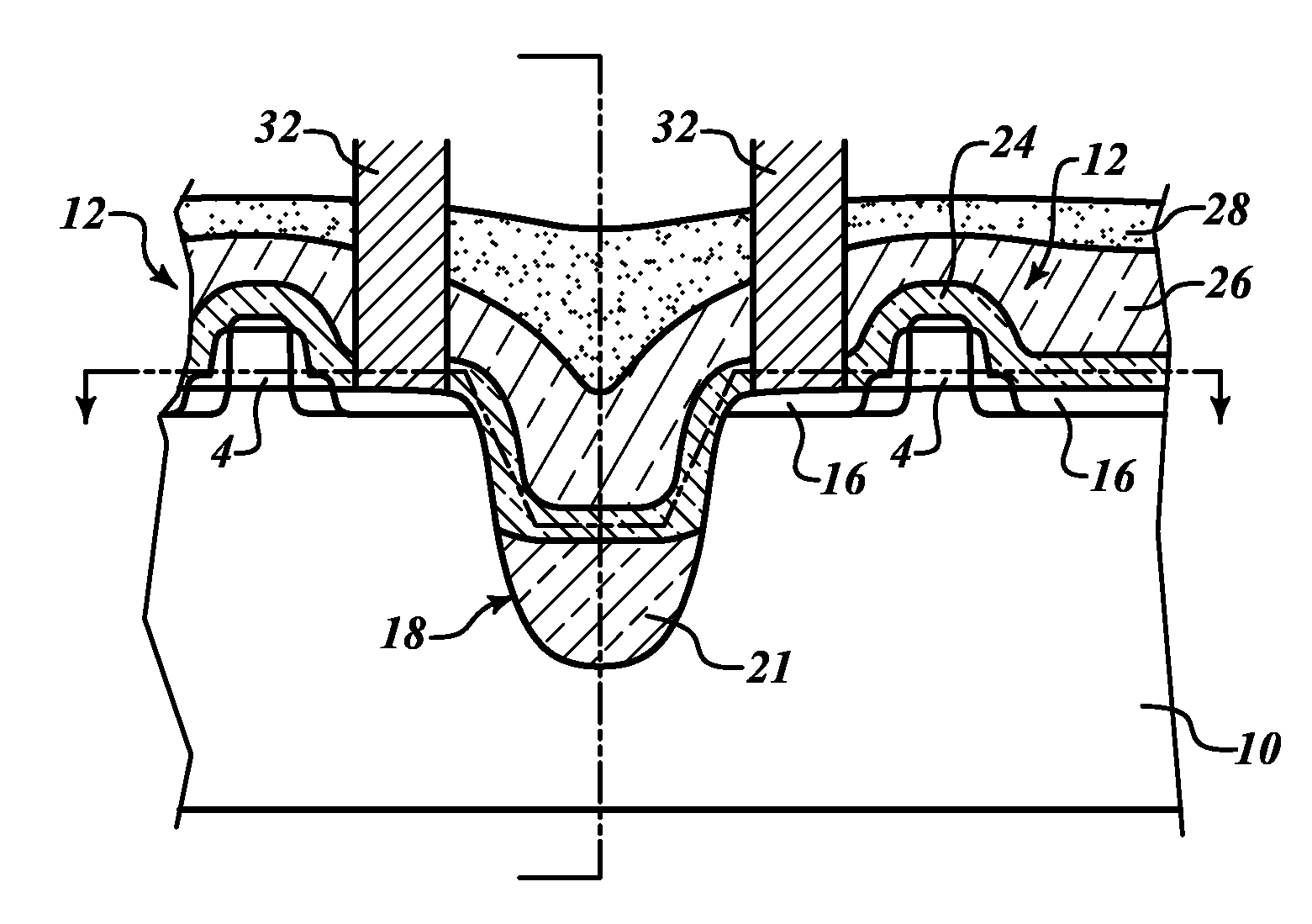
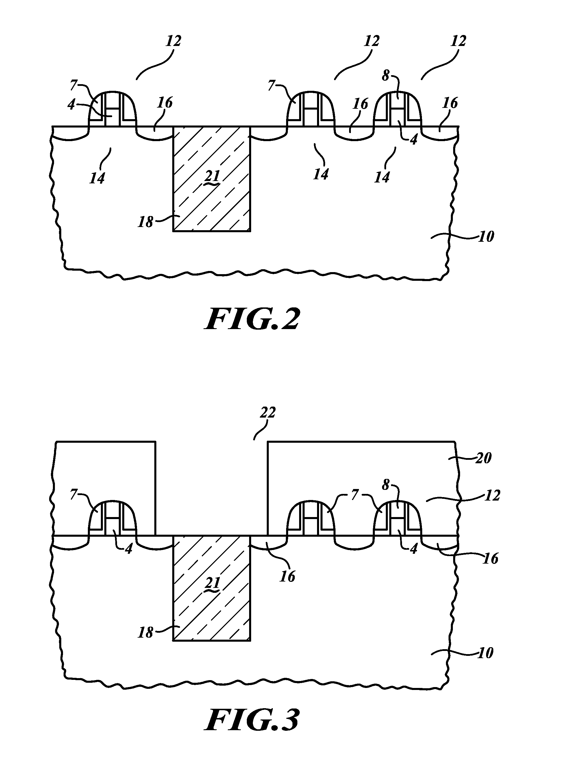
[0026]FIG. 2 illustrates a semiconductor substrate 10, preferably made of monocrystalline silicon. The substrate has a plurality of transistors 12 formed therein. The transistors include channel regions 14 and source drain / regions 16. The term source / drain region includes both the source and the drain of a MOS transistor. As is known, a heavily doped conductive region adjacent a gate electrode can be either a source or a drain, depending on the relative electrical potentials at the gate electrode. Thus, the general term source / drain region as used herein includes all such regions, whether acting as sources or drains. The transistors 12 may have LDD implants, halo regions, and other structures, as are well-known in the art.

[0027]A trench isolation region 18 electrically isolates at least two of the transistors from each other. In one embodiment, the trench isolation region 18 is filled with a dielectric material 21, which has been previously deposited according to known techniques fo...


PUM


Abstract

According to one embodiment, a semiconductor substrate is provided having at least two transistor regions formed therein. Overlying the channel regions is a gate dielectric and transistor gate electrodes overly the gate dielectric and are positioned overlying the channel regions. Source and drain regions are formed on either side of the channel regions to create a transistor structure. In order to provide isolation between transistors in the semiconductor substrate, a trench is formed in the substrate. A strain-inducting layer is then deposited over the transistor structures and into the trench in the semiconductor substrate. A high-stress nitride layer is one type of material which is suitable for forming the strain-inducing layer.

Description

RELATED APPLICATION[0001]This application claims the benefit of U.S. Provisional Application No. 61 / 142,066 filed on Dec. 31, 2008, entitled Method and Structure for Forming Strained Transistor and 61 / 168,484 entitled Method and Structure for Forming Strained Transistor, filed Apr. 10, 2009, both of which applications are incorporated herein by reference.TECHNICAL FIELD[0002]This invention relates to a method and structure for forming strained transistors and, in particular, a strain-inducing layer which overlays the transistors and is also within a trench in the semiconductor substrate for creating a strained transistor structure.BACKGROUND[0003]It is known in the art that a transistor subjected to different types of stress increases the mobility of the charge carriers in the channel region. For example, creating a tensile stress in the channel region increases the mobility of electrons and, depending on the magnitude of the stress, increases in mobility of up to 20% may be obtaine...

Claims


Application Information

Patent Timeline
Patent Type & Authority Patents(United States)
IPC IPC(8): H01L21/762H01L27/088
CPCH01L21/823412H01L21/823481H01L29/6659H01L29/7833H01L29/7843
Inventor DOVE, BARRY
Owner STMICROELECTRONICS SRL
Learn More