
Silicon carbide semiconductor substrate and method of manufacturing the same

a technology of silicon carbide and semiconductor substrate, which is applied in the direction of basic electric elements, electrical apparatus, semiconductor devices, etc., can solve problems such as unsuitability, and achieve the effect of improving conversion efficiency and reducing the dislocation density of the basal plan

Inactive Publication Date: 2012-06-19
HITACHI CABLE
View PDF6 Cites 1 Cited by
  • Summary
  • Abstract
  • Description
  • Claims
  • Application Information

AI Technical Summary

Benefits of technology

"The present invention provides a method for reducing basal plane dislocation in the epitaxial layer of a silicon carbide semiconductor substrate without negatively affecting the film quality of the epitaxial layer. By forming a dislocation conversion layer made of silicon carbide with high conversion efficiency converting basal plane dislocation into threading edge dislocation, the basal plane dislocation density in the epitaxial layer is reduced. However, the method may not be suitable for all semiconductor devices, as it may deteriorate the turn-on state reliability of the device."

Problems solved by technology

This is considered to be caused by the occurrence of separate crystal defects around the concave parts since the epitaxial layer is grown on the wafer having the concave parts.
As such, the method of forming concave parts by selectively performing etching on a part of the basal plane dislocation exposed on the surface of the silicon carbide single crystal wafer and growing the epitaxial layer on the silicon carbide single crystal wafer having the concave part formed thereon is suitable to reduce the basal plane dislocation density, but overall, it is not suitable as the method of forming the epitaxial layer to make the semiconductor device.

Method used


Image

  • Silicon carbide semiconductor substrate and method of manufacturing the same
  • Silicon carbide semiconductor substrate and method of manufacturing the same
  • Silicon carbide semiconductor substrate and method of manufacturing the same

Examples


first embodiment

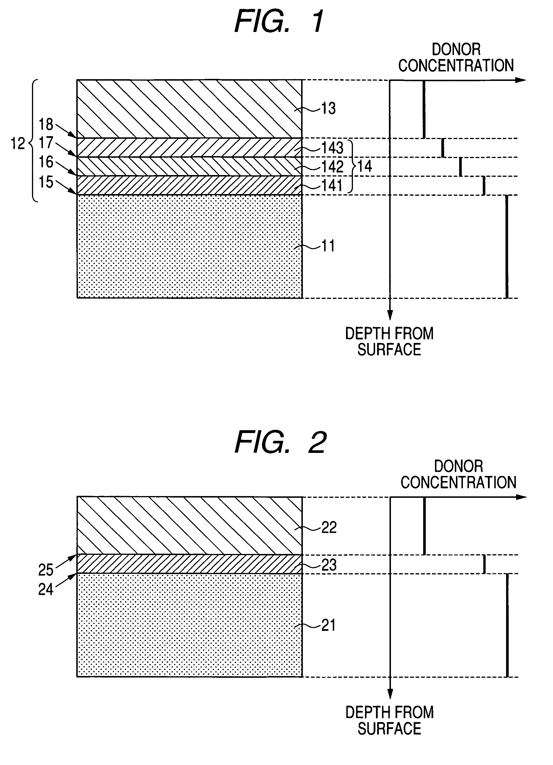
[0064]As a first embodiment of the present invention, a method of manufacturing a silicon carbide semiconductor substrate having a cross-sectional structure shown in FIG. 1 will be described.

[0065]FIGS. 5A to 5E are cross-sectional views showing a manufacturing process of a silicon carbide semiconductor substrate according to the first embodiment.

[0066]First, in the process shown in FIG. 5A, a base substrate 51 including a silicon carbide single crystal wafer is prepared. The silicon carbide single crystal wafer is an n-type 4H—SiC having a diameter of 50 mm and a (0001) Si plane inclined by 8° in a [11-20] direction, wherein donor concentration is 5×1018 cm−3. The silicon carbide single crystal wafer having a {0001} plane is a plane polarity, wherein one is a Si plane (described as a (0001) Si plane) whose outermost surface is made of silicon atoms and the other is a C plane (described as a (000-1) C plane) whose outermost surface is made of carbon atoms. The first embodiment uses ...

second embodiment

[0093]As a second embodiment of the present invention, a manufacturing method different from the first embodiment of the silicon carbide semiconductor substrate having the cross-sectional structure shown in FIG. 1 will be described.

[0094]FIGS. 8A to 8E are cross-sectional views showing a manufacturing process of a silicon carbide semiconductor substrate according to the second embodiment.

[0095]First, in the process shown in FIG. 8A, a base substrate 81 including the silicon carbide single crystal wafer is prepared. The silicon carbide single crystal wafer is the n-type 4H—SiC having a diameter of 50 mm and a (0001) Si plane inclined by 8° in a [11-20] direction, wherein the donor concentration is 5×1018 cm−3. The surface of the Si plane side of the wafer is subjected to the mechanical mirror polishing and then the CMP process.

[0096]Next, in the process shown in FIG. 8B, the base substrate 81 of FIG. 8A is subjected to an RCA cleaning and then installed in a susceptor of a reactor in...

third embodiment

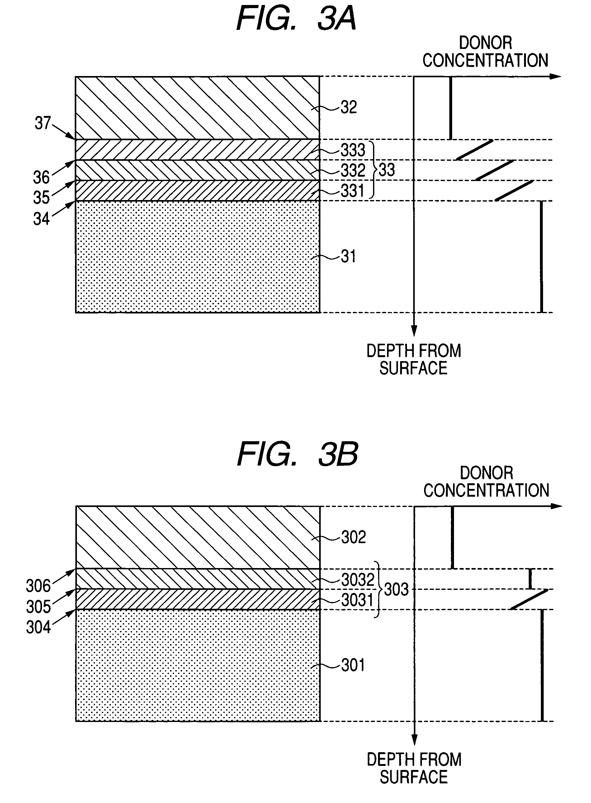
[0105]As a third embodiment of the present invention, a method of manufacturing a silicon carbide semiconductor substrate having a cross-sectional structure shown in FIG. 3A will be described.

[0106]FIGS. 9A to 9E are cross-sectional views showing a manufacturing process of a silicon carbide semiconductor substrate according to the third embodiment.

[0107]First, in the process shown in FIG. 9A, a base substrate 91 including the silicon carbide single crystal wafer is prepared. The silicon carbide single crystal wafer is the n-type 4H—SiC having a diameter of 50 mm and a (0001) Si plane inclined by 8° in a [11-20] direction, wherein the donor concentration is 5×1018 cm−3. The surface of the Si plane side of the wafer is subjected to the mechanical mirror polishing and then the CMP process. Next, in the process shown in FIG. 9B, the base substrate 91 of FIG. 9A is subjected to an RCA cleaning and then installed in a susceptor of a reactor in a hot-wall CVD system. Next, the reactor is d...


PUM

PropertyMeasurementUnit
covalent radiusaaaaaaaaaa
diameteraaaaaaaaaa

Abstract

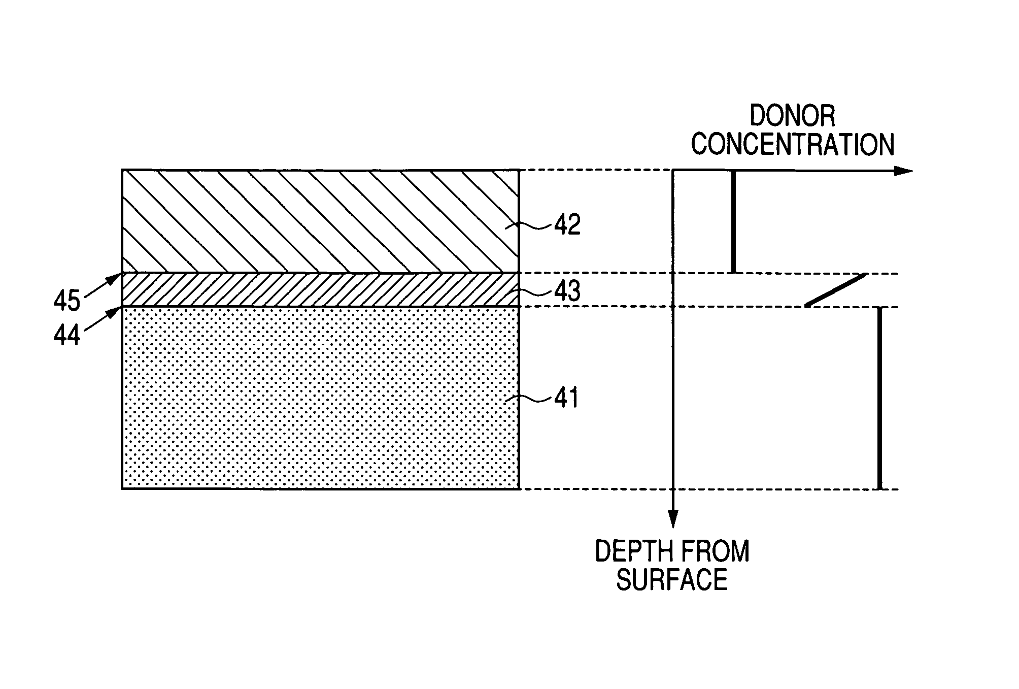
A buffer layer configured of the same conductive semiconductor layers of two or more layers as a drift layer is installed by epitaxial growth between a first semiconductor layer configuring the drift layer that is a layer in which components of the semiconductor device are made and a base substrate including a silicon carbide single crystal wafer. A step of donor concentration is provided at an interface between the drift layer and the buffer layer, an interface between the semiconductor layers configuring the buffer layer, and an interface between the buffer layer and the base substrate and the donor concentration of the drift layer side is lower than that of the base substrate side, thereby making it possible to convert most basal plane dislocations into threading edge dislocations as compared to the drift layer having one layer or the buffer layer configured of one layer.

Description

CLAIM OF PRIORITY[0001]The present application claims priority from Japanese patent application JP 2008-146711 filed on Jun. 4, 2008, the content of which is hereby incorporated by reference into this application.BACKGROUND OF THE INVENTION[0002]1. Field of the Invention[0003]The present invention relates to a silicon carbide semiconductor substrate and a method of manufacturing the same.[0004]2. Description of the Related Art[0005]Since silicon carbide (SiC) has a larger band gap and a higher electric breakdown field than silicon (Si), it is expected to be applied to a semiconductor device (power device) for next generation power control. Even though it is known that silicon carbide has many crystal structures, 4H—SiC and 6H—SiC having a hexagonal crystal structure among these crystal structures are used to manufacture a practical power device.[0006]Since there is a need to conduct a large current into a semiconductor device, many power devices have a structure where an electrode i...

Claims


Application Information

Patent Timeline
Patent Type & Authority Patents(United States)
IPC IPC(8): H01L29/24
CPCH01L21/02378H01L21/02433H01L21/02447H01L21/0262H01L21/02529H01L21/02609H01L21/02505
Inventor OHNO, TOSHIYUKIYOKOYAMA, NATSUKIGOTO, HAJIME
Owner HITACHI CABLE
Learn More