Tuner and transformer formed by printed circuit board thereof
a technology of printed circuit board and transformer, which is applied in the field of transformers, can solve the problems of reducing throughput, increasing production costs, and reducing throughput, and achieving the effect of reducing the size of the circuit and the cost of the components
- Summary
- Abstract
- Description
- Claims
- Application Information
AI Technical Summary
Benefits of technology
Problems solved by technology
Method used
Image
Examples
first embodiment
The First Embodiment
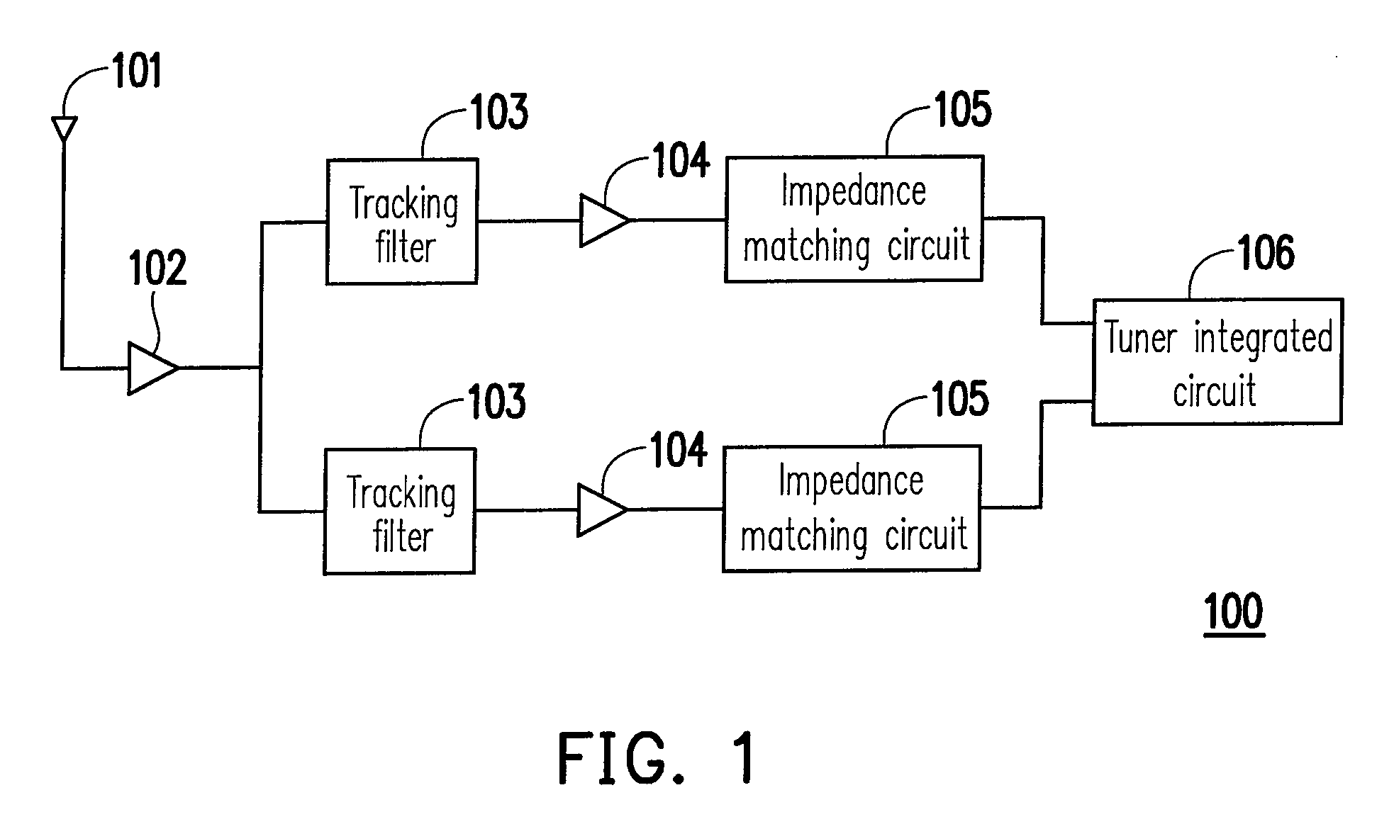
[0020]FIG. 1 is a block diagram of a tuner 100 according to an exemplary embodiment of the present invention. Referring to FIG. 1, the tuner 100 includes an antenna 101, a front-end amplifier 102, a tracking filter 103, a secondary amplifier 104, an impedance matching circuit 105 and a tuner integrated circuit 106. A transformer formed by conducting wires of a printed circuit board may be respectively applied to the tracking filter 103, the impedance matching circuit 105 and the tuner integrated circuit 106 for substituting a conventional air coil.
second embodiment
The Second Embodiment
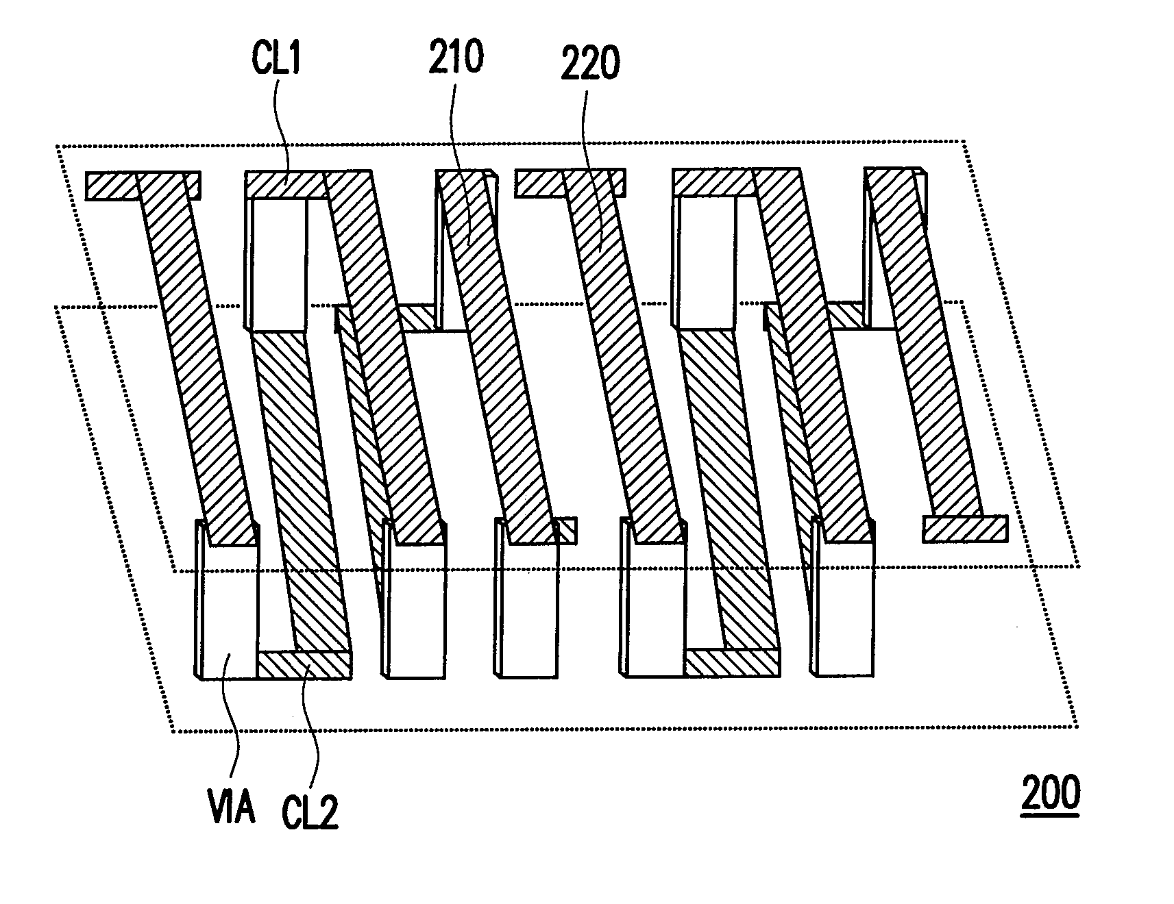
[0021]FIG. 2 is a structural diagram of a transformer according to the second embodiment of the present invention. A first winding 210 and a second winding 220 formed by conducting wires on the printed circuit board are disposed opposite to form a transformer 200. In the present embodiment, the printed circuit board has two conductor layers connected with each other by vias, for example through via, blind via or buried via. The first winding 210 and the second winding 220 may form a rectangular winding through the two conductor (metal) layers (for example, CL1, CL2) and the VIAs, as shown in FIG. 2.
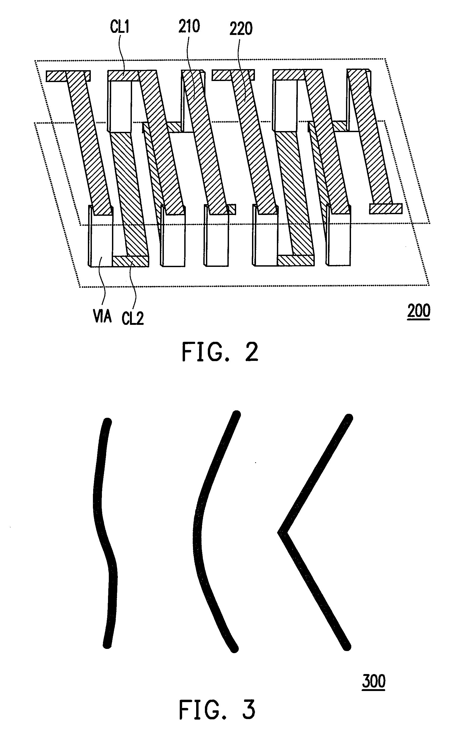
[0022]The layout of the first winding 210 and the second winding 220 are not limited to a rectangle, which may also be an arc or a triangle, as shown in FIG. 3. FIG. 3 is a diagram illustrating different layout patterns of conducting wires according to the first embodiment. The first winding 210 and the second winding 220 may have different designs of the conductor la...
third embodiment
The Third Embodiment
[0025]FIG. 4 is a circuit diagram of an impedance matching circuit according to the third embodiment of the present invention. The impedance matching circuit 400 includes the transformer 200, a first matching circuit 410 and a second matching circuit 420. The first matching circuit 410 includes a resistor R31, a varactor D31, a compensation inductor L31 and a capacitor C32. The second matching circuit 420 includes a resistor R32, a varactor D32, a compensation inductor L32 and a capacitor C33. The transformer 200 is formed by conducting wires of the printed circuit board, and has a structure similar to that shown in FIG. 2. The first end P1 and the second end P2 are two ends of the first winding, the third end P3 and the fourth end P4 are two ends of the second winding. The description with reference to FIG. 2 may be referred for a detailed layout of the transformer 200.
[0026]The capacitor C31 is coupled between the first end P1 and a signal input terminal IN, an...
PUM
 Abstract
Description
Claims
Application Information
 - R&D
- Intellectual Property
- Life Sciences
- Materials
- Tech Scout
- Unparalleled Data Quality
- Higher Quality Content
- 60% Fewer Hallucinations
Browse by: Latest US Patents, China's latest patents, Technical Efficacy Thesaurus, Application Domain, Technology Topic, Popular Technical Reports.
© 2025 PatSnap. All rights reserved.Legal|Privacy policy|Modern Slavery Act Transparency Statement|Sitemap|About US| Contact US: help@patsnap.com


