
Semiconductor device

a technology of electromagnetic field and semiconductor device, which is applied in the direction of burglar alarm mechanical actuation, burglar alarm by hand-portable object removal, instruments, etc., can solve the problems of difficult to increase the process yield, low reliability, and inability to detect in a connection portion easily caused, so as to achieve small coercivity, increase mutual inductance of antennas, and high permeability

Active Publication Date: 2012-04-17
SEMICON ENERGY LAB CO LTD
View PDF25 Cites 10 Cited by
  • Summary
  • Abstract
  • Description
  • Claims
  • Application Information

AI Technical Summary

Benefits of technology

[0007]The present invention has been made in view of the above described problems. It is an object of the present invention to provide an ID chip in which gain of an antenna is increased and the mechanical strength of an integrated circuit can be enhanced without suppressing a circuit scale. Further, the present invention relates to a packing material, a tag, a certificate, a bank note, a portfolio and the like using the ID chip.
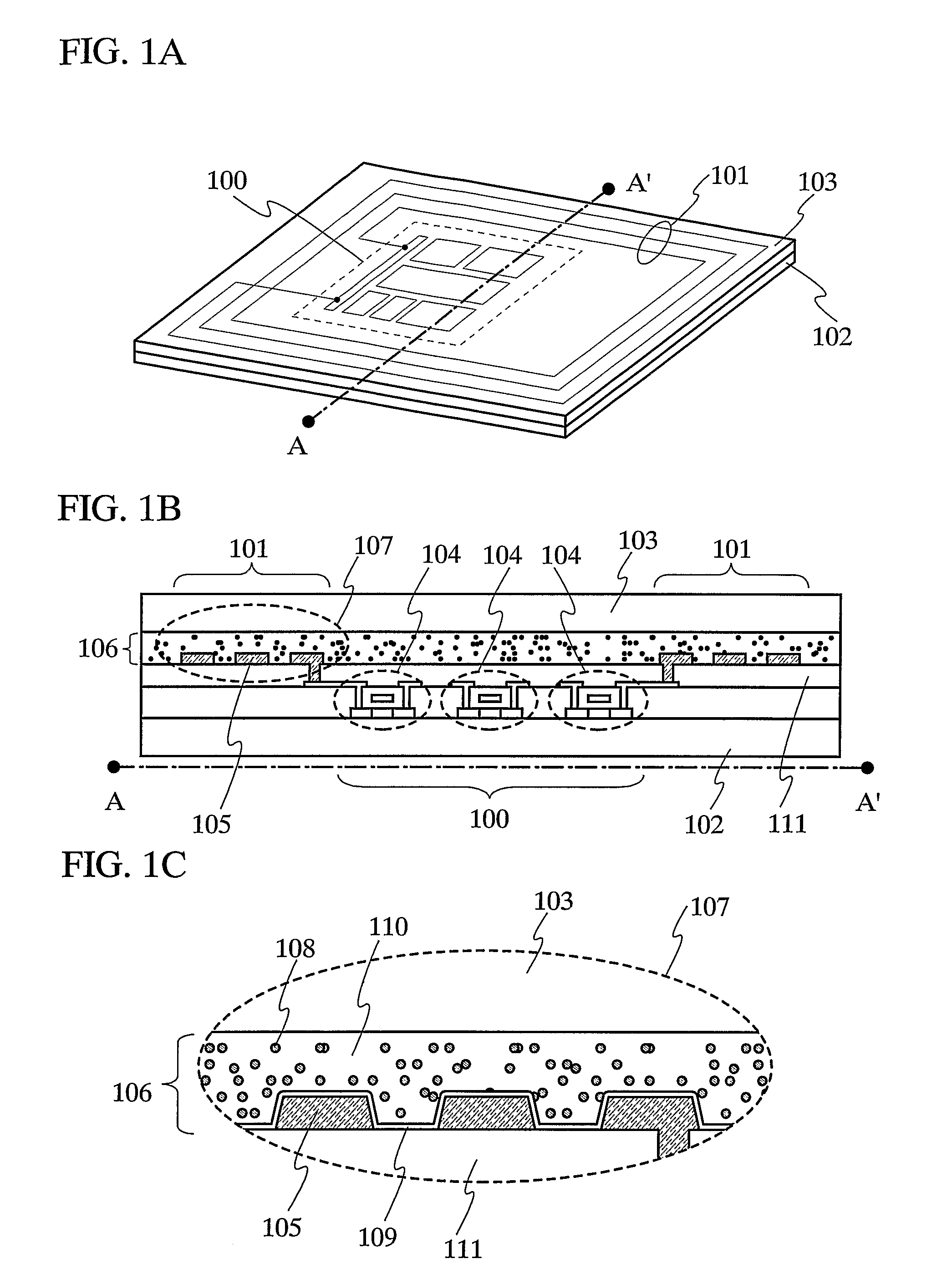
[0012]Integrated circuits, which are formed separately, may be attached to one another to stack the integrated circuits such that the scale of the circuits or the memory capacity may be increased. Since the integrated circuits are dramatically thin in thickness as compared with an ID chip manufactured using a semiconductor substrate, the mechanical strength of an ID chip can be maintained to some extent even when the plural integrated circuits are stacked. The stacked integrated circuits can be connected to one another by using a known connection method such as a flip chip method, a TAB (tape automated bonding) method or a wire bonding method.
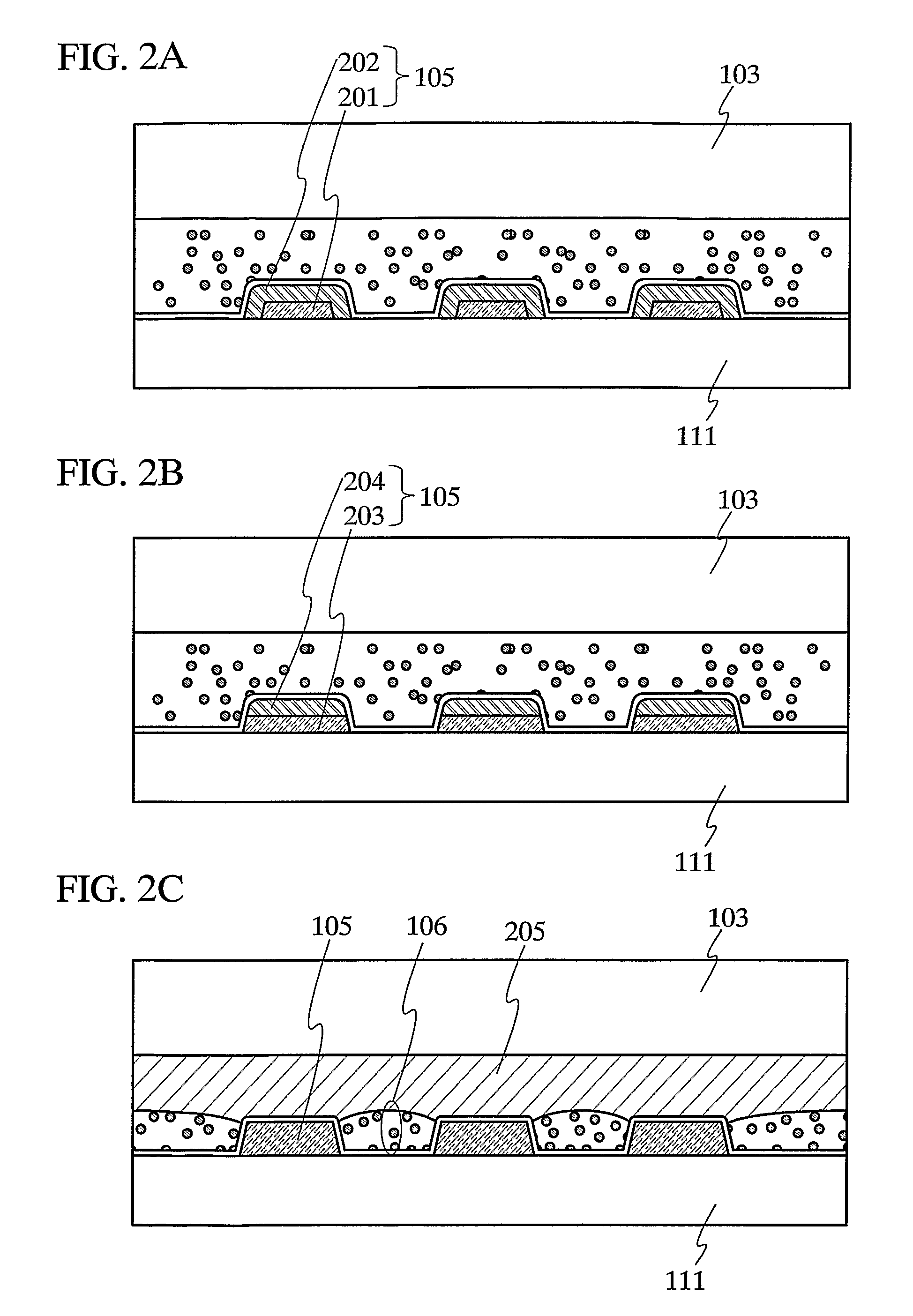
[0014]The soft magnetic material is a magnetic material that has high permeability and small coercitivity. Therefore, it is preferable that the soft magnetic material is arranged between conducting wires, and generation of eddy current in a conductor of the conducting wires, due to a magnetic flux that intersects with a plane including an antenna, would be suppressed. Accordingly, it is preferable that the loss of the magnetic flux that intersects with a plane including an antenna is suppressed, and the mutual inductance of the antenna would be increased. It is preferable that the gain of the antenna would be increased while securing the mechanical strength of the ID chip.
[0015]An insulating film including a soft magnetic material is formed to cover the conductive wires. Thus, it is preferable to prevent the magnetic flux which is generated in the antenna from being lost by the conductors arranged in the vicinity of the conducting wires. Specifically, when a conductor is used for a surface of an object to which an ID chip is attached, the ID chip is attached such that an insulating layer including a soft magnetic material is arranged between the antenna and the surface. At this time, it is preferable to prevent the loss of magnetic flux due to the conductor.
[0016]A wiring for connecting an integrated circuit and an antenna can be formed over the substrate in the process of manufacturing the integrated circuit, by forming the integrated circuit and the antenna integrally. Therefore, generation of connection failure in forming an ID chip can be reduced. Further, when a flexible substrate is used, a connection failure due to application of stress to a substrate can be also reduced and thus the reliability is enhanced.
[0017]A flexible substrate can be used since an integrated circuit is formed by using a semiconductor element formed from a thin semiconductor film. It is preferable to obtain the high mechanical strength without reducing the area, different from an integrated circuit using a semiconductor substrate. Therefore, it is preferable to enhance the mechanical strength of an integrated circuit without reducing the circuit scale and to enlarge the application range of an ID chip.

Problems solved by technology

As for the ID chip formed by connecting an integrated circuit and an antenna, which have been formed separately, defects are easily caused in the connection portion of the integrated circuit and the antenna, and thus it is difficult to increase the process yield.
Thus, there is a problem that defects are caused easily by the stress and thus, the reliability is low.
On the other hand, in an ID chip where an integrated circuit and an antenna are formed integrally, such a detect in a connection portion is not easily caused, different from one where an integrated circuit and an antenna are formed separately.
However, the area for forming an antenna is naturally limited if the number of ID chips formed from one substrate is to be secured.
Thus, it is difficult to enlarge the size of an antenna and to form a high gain antenna.
A semiconductor substrate used for forming an integrated circuit is generally poor in flexibility and mechanical strength, which is a drawback.
However, the case is not favorable, since securing a circuit scale is difficult and the use of an ID chip is limited.
Therefore, it is not favorable that the area of an integrated circuit is randomly reduced when securing the circuit scale of the integrated circuit is considered to be important.

Method used


Image

  • Semiconductor device
  • Semiconductor device
  • Semiconductor device

Examples


embodiment 2

[0148]Embodiment 2 describes one mode of a functional configuration of a semiconductor device such as an ID chip according to the present invention with reference to FIG. 11.

[0149]In FIG. 11, reference numeral 900 denotes an antenna, 901 denotes an integrated circuit, and 903 denotes a capacitor formed between both terminals of the antenna 900. The integrated circuit 901 includes a demodulation circuit 909, a modulation circuit 904, a rectification circuit 905, a microprocessor 906, a memory 907, and a switch 908 for providing load modulation to the antenna 900. In addition, the number of the memory 907 is not limited to one; a plurality of the memories 907 may be provided. As the memory 907, a SRAM, a flash memory, a ROM, a FRAM (registered mark), or the like may be used.

[0150]A signal sent from the reader / writer as a radio wave is converted into an alternating electric signal by electromagnetic induction in the antenna 900. The alternating electric signal is demodulated in the dem...

embodiment 3

[0154]Embodiment 3 describes a structure of a TFT used in a semiconductor device such as an ID chip of the present invention.

[0155]FIG. 12A shows a cross sectional view of TFT according to the embodiment. Reference numeral 701 represents an n-channel TFT; and 702, a p-channel TFT. The configuration of the n-channel TFT 701 will be explained in detail as an example.

[0156]The n-channel TFT 701 includes an island-like semiconductor film 705 to be used as an active layer. The island-like semiconductor film 705 includes two impurity regions 703 to be used as a source region and a drain region, a channel formation region 704 sandwiched between the two impurity regions 703, and two LDD (lightly doped drain) regions 710 sandwiched between the impurity regions 703 and the channel formation region 704. The n-channel TFT 701 further includes a gate insulating film 706 covering the island-like semiconductor film 705, a gate electrode 707, and two sidewalls 708 and 709 made from insulating films...

embodiment 4

[0169]In this embodiment, a method for manufacturing plural semiconductor devices such as ID chips with the use of a large size substrate will be described.

[0170]An integrated circuit 401 and an antenna 402 are formed over a heat resistant substrate. Thereafter, the integrated circuit 401 and the antenna 402 are both separated from the heat resistant substrate and attached to a substrate 403, which has been separately prepared, with an adhesive agent 404 as shown in FIG. 13A. Although FIG. 13A shows a mode in which a set of the integrated circuit 401 and the antenna 402 is attached to the substrate 403, the present invention is not limited to this configuration. Alternatively, a plurality of sets of the integrated circuit 401 and the antenna 402, which are connected to each other, may be separated from the heat resistant substrate and attached onto the substrate 403 at the same time.

[0171]As shown in FIG. 13B, a cover material 405 is attached to the substrate 403 such that the integ...


PUM


Abstract

A semiconductor device such as an ID chip of the present invention includes an integrated circuit using a semiconductor element formed by using a thin semiconductor film, and an antenna connected to the integrated circuit. It is preferable that the antenna is formed integrally with the integrated circuit, since the mechanical strength of an ID chip can be enhanced. Note that the antenna used in the present invention also includes a conducting wire that is wound round circularly or spirally and fine particles of a soft magnetic material are arranged between the conducting wires. Specifically, an insulating layer in which fine particles of a soft magnetic material are arranged between the conducting wires. Specifically, an insulating layer in which fine particles of a soft magnetic material are included is arranged between the conducting wires.

Description

TECHNICAL FIELD[0001]The present invention relates to a semiconductor device that can conduct wireless communication.BACKGROUND ART[0002]A semiconductor device such as an ID chip that can transmit and receive data such as identification information wirelessly has been coming into practical use in various areas, and the expansion of its market is further anticipated as a communication information terminal of a new mode. An ID chip is called also a wireless tag, a RFID (Radio frequency identification) tag or an IC tag, and one having an antenna and an integrated circuit formed by using a semiconductor substrate is coming into practical use at present.DISCLOSURE OF INVENTION[0003]The category of ID chips includes an ID chip formed by connecting an integrated circuit and an antenna, which have been formed separately, and an ID chip formed by sequentially (integrally) forming an integrated circuit and an antenna on the same substrate.[0004]As for the ID chip formed by connecting an integ...

Claims


Application Information

Patent Timeline
Patent Type & Authority Patents(United States)
IPC IPC(8): H01L21/08G06K19/07G06K19/077H01L21/77H01L21/8234H01L27/04H01L27/06H01L27/12H01L27/13H01L29/786H01Q1/22H01Q1/38H01Q7/00H01Q23/00
CPCG06K19/07749G06K19/07775G06K19/07779H01L27/12H01L27/13H01Q1/2208H01Q1/38H01Q23/00H01L27/1214H01L27/1266H01Q1/2283G06K19/07G06K19/077H01L21/70H01L21/8234
Inventor YAMAZAKI, SHUNPEIARAO, TATSUYA
Owner SEMICON ENERGY LAB CO LTD
Learn More