Thin-film photovoltaic structures including semiconductor grain and oxide layers

a photovoltaic structure and thin film technology, applied in the field of photovoltaics, can solve the problems of excess kinetic energy, esub>k/sub>(excess) loss, and efficiency to 31%, and achieve the effect of low cos

Inactive Publication Date: 2012-04-17
ZETTA RES & DEV LLC - AQT SERIES
View PDF31 Cites 18 Cited by
  • Summary
  • Abstract
  • Description
  • Claims
  • Application Information

AI Technical Summary

Benefits of technology

[0014]The properties of the semiconductor grains can be controlled, and in some instances varied, to achieve a variety of effects and advantages. For example, the size of the semiconductor grains can be configured to facilitate extraction of charge carriers before they can relax to the band edge, increasing the efficiency of the photon conversion in nanometer sized semiconductor absorbers. In addition, the size and / or composition of the semiconductor grains in multiple semiconductor and oxide layers can be varied to match the band gap energies of the semiconductor grains to the solar energy spectrum. This can further reduce the energy loss due to the relaxation of carriers to their respective band edges. The composition of the semiconductor grains can also be varied. For example, one or more of the semiconductor and oxide layers may contain gold (Au).

Problems solved by technology

A significant factor limiting the conversion efficiency to 31% is that the excess kinetic energy (absorbed photon energy above the semiconductor band gap energy) Ek(excess) is lost as heat through electron-phonon scattering.
The diffusion of carriers does not happen indefinitely, however, because of an opposing electric field created by this charge imbalance.
A noted drawback of both dye-sensitized and quantum dot-sensitized solar cells is long term stability due to the presence of electrolyte.
Therefore the material cannot be used, without some modification, in solar cells.

Method used


Image

  • Thin-film photovoltaic structures including semiconductor grain and oxide layers
  • Thin-film photovoltaic structures including semiconductor grain and oxide layers
  • Thin-film photovoltaic structures including semiconductor grain and oxide layers

Examples


Embodiment Construction

A. Overview

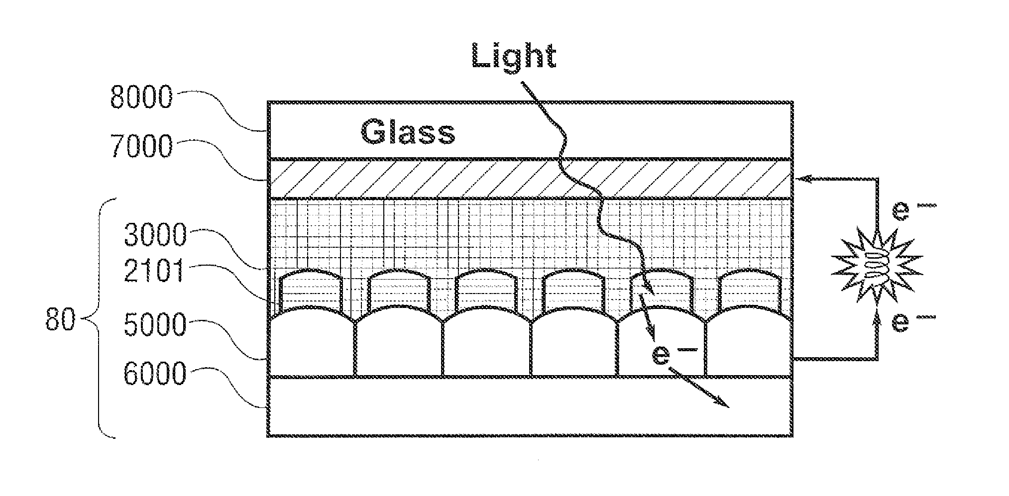
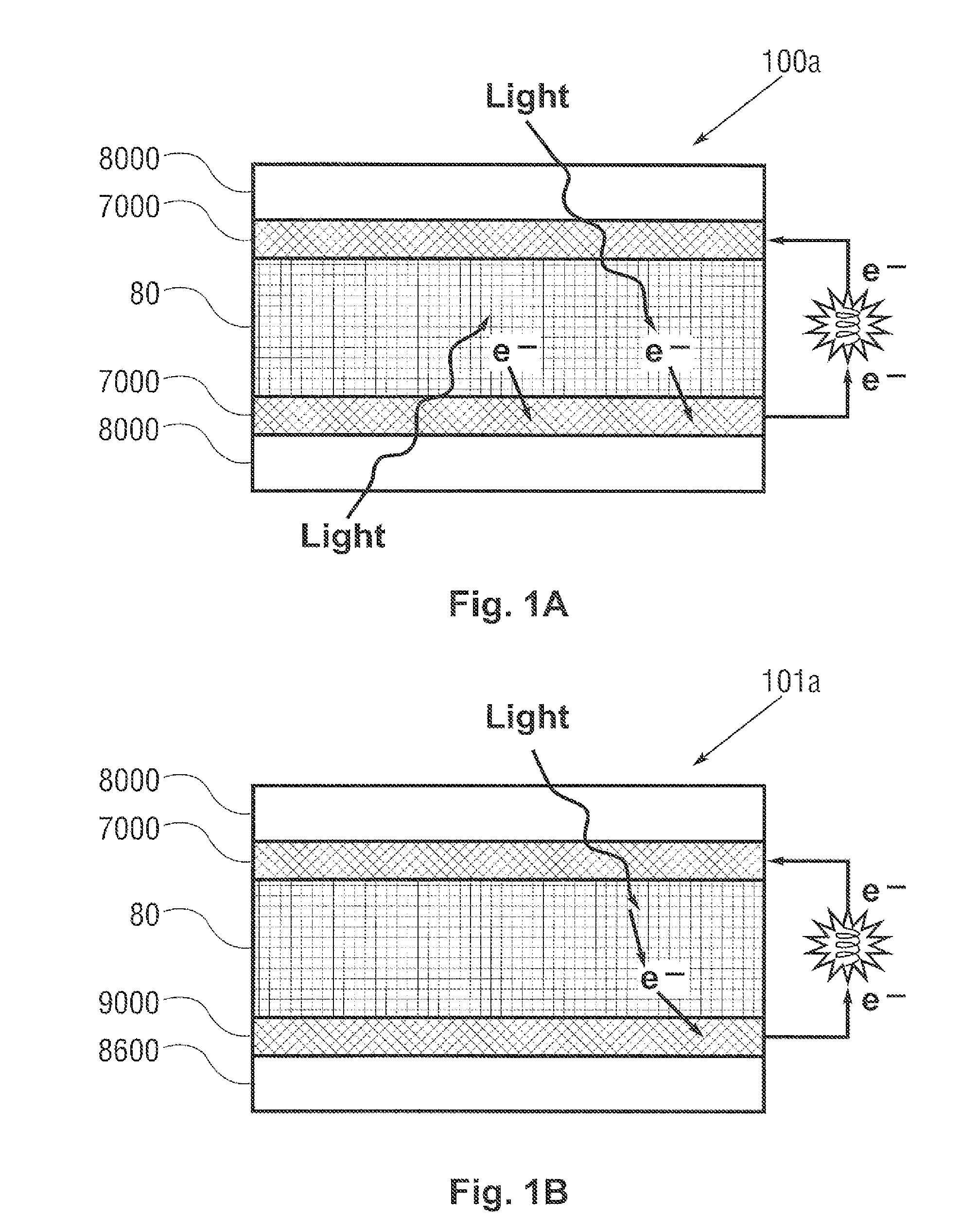
[0024]FIGS. 1a to 1d illustrate example structures and configurations of solar cells according to several possible implementations of the invention. As FIG. 1a illustrates, a solar cell 100a may comprise, in overlying sequence a transparent layer 8000, a transparent conductive layer 7000, a photoactive conversion layer 80, a second transparent conductive layer 7000 and a second transparent material layer 8000. In a particular implementation, the transparent conductive layer 7000 may be indium oxide doped with tin oxide. In some implementations, the transparent layer 8000 may be glass, plastic or other suitable protective material.

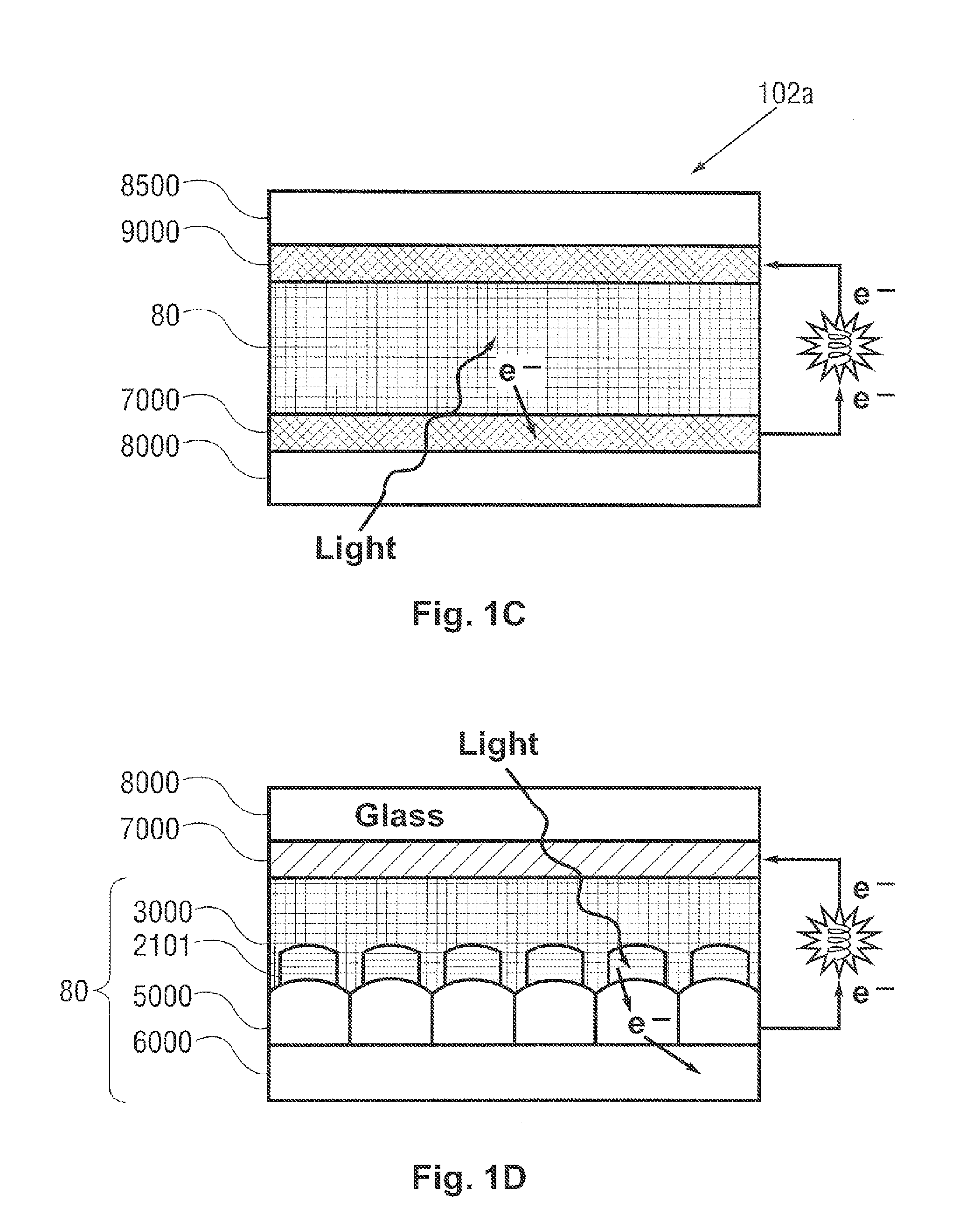
[0025]In other implementations, solar cell 101a, as FIG. 1b shows, may comprise (in overlying sequence) non-transparent substrate 8600, contact layer 9000, photoactive conversion layer 80, transparent conductive layer 7000, and transparent material layer 8000. FIG. 1c shows solar cell 102a comprising (in overlying sequence) transparent substrate ...


PUM

PropertyMeasurementUnit
band gap energiesaaaaaaaaaa
semiconductor band gap energyaaaaaaaaaa
sizesaaaaaaaaaa

Abstract

Photovoltaic structures for the conversion of solar irradiance into electrical free energy. In a particular implementation, a photovoltaic cell includes a granular semiconductor and oxide layer with nanometer-size absorber semiconductor grains surrounded by a matrix of oxide. The semiconductor and oxide layer may be disposed between electron and hole conducting layers. In some implementations, multiple semiconductor and oxide layers can be deposited.

Description

CROSS-REFERENCE TO RELATED APPLICATION(S)[0001]The present application is a continuation-in-part of U.S. application Ser. No. 11 / 923,036, filed Oct. 24, 2007, and a continuation-in-part of U.S. application Ser. No. 11 / 923,070, filed Oct. 24, 2007, both of which are incorporated by reference herein in their entirety for all purposes. The present application also claims priority to U.S. Provisional Application Ser. No. 60 / 881,013, filed Jan. 17, 2007.TECHNICAL FIELD[0002]The present disclosure generally relates to photovoltaics.BACKGROUND[0003]The maximum thermodynamic efficiency for the conversion of non-concentrated solar irradiance into electrical free energy for a single-band semiconductor absorber is approximately 31 percent [W. Shockley, H. J. Queisser, J., Appl. Phys., 32, 510 (1961)]. This efficiency is attainable in semiconductors with band gap energies ranging from 1.25 to 1.45 electronvolts (eV). For semiconductors, band gap generally refers to the energy difference between...

Claims


Application Information

Patent Timeline
Patent Type & Authority Patents(United States)
IPC IPC(8): H01L31/00H01L27/14
CPCB82Y20/00B82Y30/00H01L31/032H01L31/0352H01L31/0384H01L31/072H01L31/075H01L31/18H01L51/0037H01L51/426H01L51/4293Y02E10/548Y10S977/954Y10S977/948Y10S977/712Y10S977/778Y10S977/72H10K85/1135H10K30/35H10K30/40
Inventor GIRT, EROLMUNTEANU, MARIANA RODICA
Owner ZETTA RES & DEV LLC - AQT SERIES
Why Eureka
Try Eureka