Display device and method of manufacturing the same
a technology of display device and manufacturing method, which is applied in the direction of radio frequency controlled devices, semiconductor devices, electrical apparatus, etc., can solve the problems of increasing reducing worsening the delay of electrode wires due to impedance, so as to reduce the number of photomasks and the resistance of conductive wires, increase the signal transmission speed of display device, and reduce manufacturing costs
- Summary
- Abstract
- Description
- Claims
- Application Information
AI Technical Summary
Benefits of technology
Problems solved by technology
Method used
Image

Examples
first embodiment
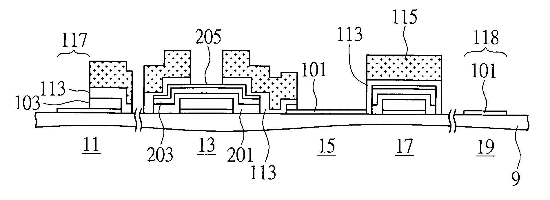
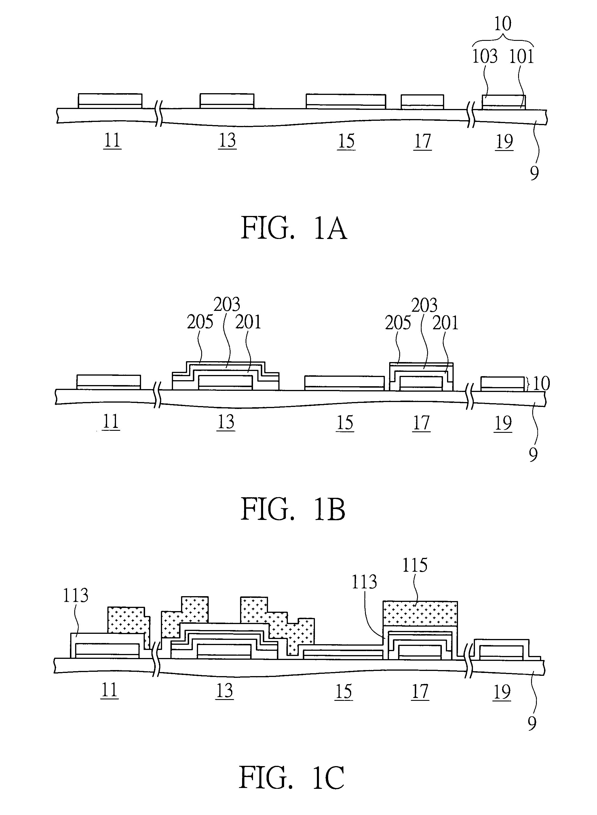
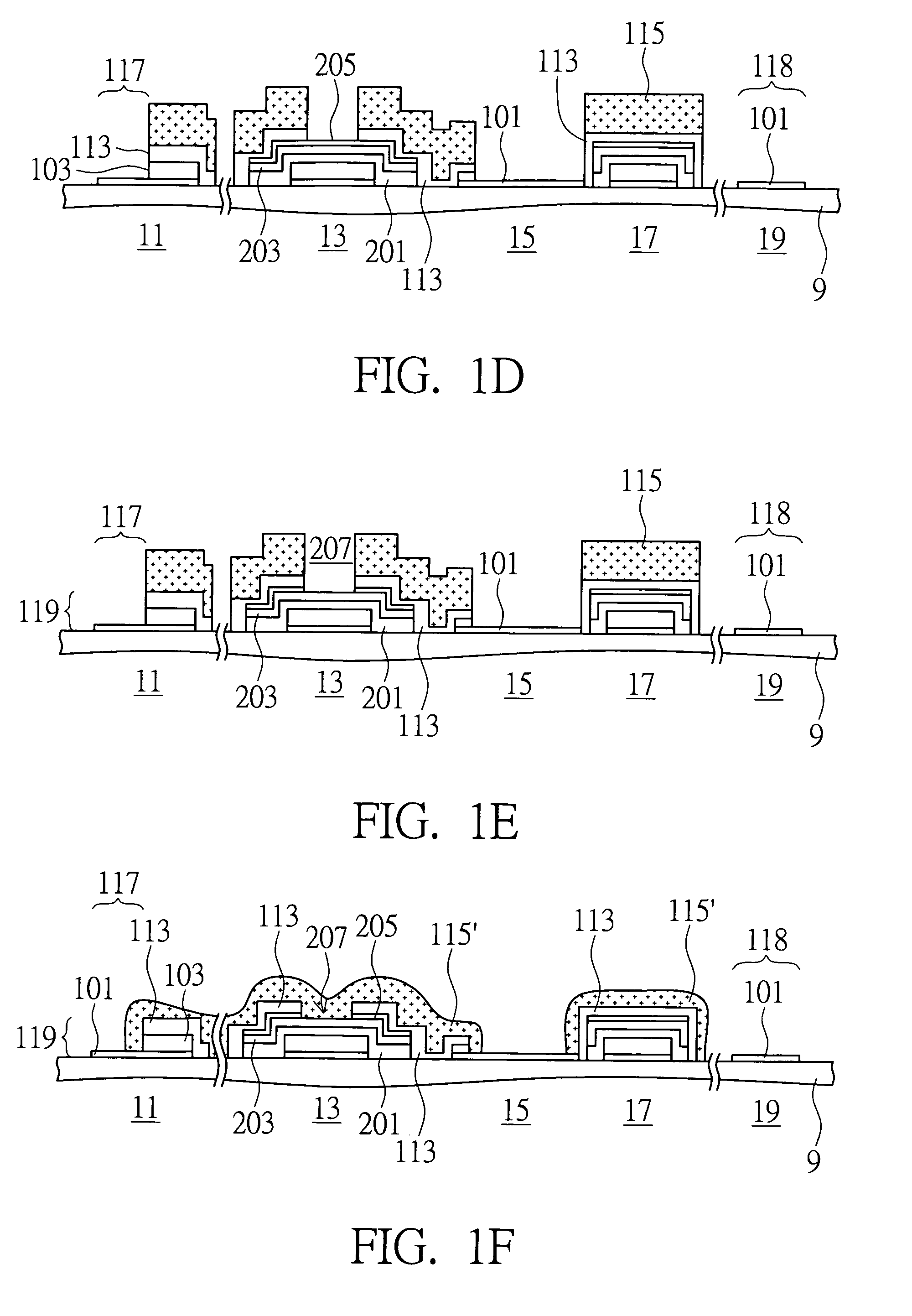
[0021]Referring to FIGS. 1A˜1F, diagrams illustrating a method of manufacturing a display device according to a first embodiment of the present invention are shown. Referring to FIGS. 2A˜2C, top views of FIGS. 1A, 1B and 1F are shown. FIGS. 1A, 1B and 1F are cross-sectional view along the cross-sectional line L-L′ of FIGS. 2A˜2C.
[0022]The display device comprises a plurality of scan signal lines (not illustrated) and a plurality of data signal lines (not illustrated), wherein the scan signal lines and the data signal lines are criss-crossed in a matrix form, a plurality of pixels are defined by the scan signal lines and the data signal lines, and each pixel is defined by a pair of neighboring scan signal lines and a pair of neighboring data signal lines. To elaborate the manufacturing method of the present embodiment, each pixel comprises a gate-line region 11, a TFT region 13, a pixel region 15, a capacitor region 17 and a data-line region 19.
The First Photomask Process
[0023]Referr...
second embodiment
[0036]The capacitor structure of the second embodiment is different from that of the first embodiment. As part of the manufacturing process in the method of manufacturing display device according to the second embodiment is similar to that according to the first embodiment, the similarities are referred to FIGS. 1A˜1F and related elaboration and are not repeated here.
[0037]Referring to FIG. 3, one step of a method of manufacturing a display device according to a second embodiment of the present invention is shown. In the second embodiment, the conductive stack layer 10 is formed within each of the TFT region 13, the pixel region 15, the capacitor region 17, the gate-line region 11 and the end of the data-line region 19 as indicated in FIG. 1A. Then, a patterned first insulating layer 201 and a patterned semiconductor layer 203 (and a patterned Ohm contact layer 205) are formed within the TFT region 13, and a patterned first insulating layer 201 is concurrently formed on the capacito...
third embodiment
[0042]In the first embodiment and the second embodiment, the TFT structure of the display device is exemplified by back channel etching (BCE) TFT, but in the third embodiment, the TFT structure of the display device is exemplified by etch stop type (I-Stop) TFT.
[0043]Referring to FIG. 6A˜FIG. 6G, diagrams illustrating a method of manufacturing a display device according to a third embodiment of the present invention are shown. Also, referring to FIGS. 7A˜7C, respective top views of FIG. 6A, FIG. 6B and FIG. 6G are shown. FIG. 6A, FIG. 6B and FIG. 6G are cross-sectional views along the cross-sectional lines L-L′ of FIG. 7A˜FIG. 7C.
[0044]The display device comprises a plurality of scan signal lines (not illustrated) and a plurality of data signal lines (not illustrated), wherein the scan signal lines and the data signal lines are criss-crossed in a matrix form, a plurality of pixels are defined by the scan signal lines and the data signal lines, and each pixel is defined by a pair of ...
PUM
 Abstract
Description
Claims
Application Information
 - R&D
- Intellectual Property
- Life Sciences
- Materials
- Tech Scout
- Unparalleled Data Quality
- Higher Quality Content
- 60% Fewer Hallucinations
Browse by: Latest US Patents, China's latest patents, Technical Efficacy Thesaurus, Application Domain, Technology Topic, Popular Technical Reports.
© 2025 PatSnap. All rights reserved.Legal|Privacy policy|Modern Slavery Act Transparency Statement|Sitemap|About US| Contact US: help@patsnap.com