
Methods for forming resistive switching memory elements by heating deposited layers

a resistive switching and memory element technology, applied in the field of nonvolatile memory elements, can solve the problems of multilayer materials that undergo high temperature treatment, affecting the processing efficiency of multilayer materials, and posing challenges for traditional nonvolatile memory technology, so as to reduce the complexity of the process

Active Publication Date: 2012-03-27
INTERMOLECULAR
View PDF20 Cites 93 Cited by
  • Summary
  • Abstract
  • Description
  • Claims
  • Application Information

AI Technical Summary

Benefits of technology

This method enhances the formation of resistive switching structures with improved interfacial integrity and avoids undesirable oxidation, leading to more reliable and efficient nonvolatile memory elements with bistable resistance states suitable for digital data storage.

Problems solved by technology

However, as device dimensions shrink, scaling issues are posing challenges for traditional nonvolatile memory technology.
Arrangements such as these may be satisfactory, but can give rise to processing challenges.
For example, multilayer materials that undergo high temperature treatments may lose interfacial integrity due to interdiffusion or stress-induced delamination.
Moreover, the use of conventional rapid thermal oxidation processes or other such post-processing oxidation techniques to form resistive switching metal oxide films may lead to undesirable oxidation of contact pads or other device features.

Method used


Image

  • Methods for forming resistive switching memory elements by heating deposited layers
  • Methods for forming resistive switching memory elements by heating deposited layers
  • Methods for forming resistive switching memory elements by heating deposited layers

Examples


Embodiment Construction

[0027]A detailed description of one or more embodiments is provided below along with accompanying figures. The detailed description is provided in connection with such embodiments, but is not limited to any particular example. The scope is limited only by the claims and numerous alternatives, modifications, and equivalents are encompassed. Numerous specific details are set forth in the following description in order to provide a thorough understanding. These details are provided for the purpose of example and the described techniques may be practiced according to the claims without some or all of these specific details. For the purpose of clarity, technical material that is known in the technical fields related to the embodiments has not been described in detail to avoid unnecessarily obscuring the description.

[0028]Embodiments of the present invention relate to nonvolatile memory formed from resistive switching elements. Embodiments of the invention also relate to fabrication metho...


PUM

PropertyMeasurementUnit
temperatureaaaaaaaaaa
length of timeaaaaaaaaaa
temperatureaaaaaaaaaa

Abstract

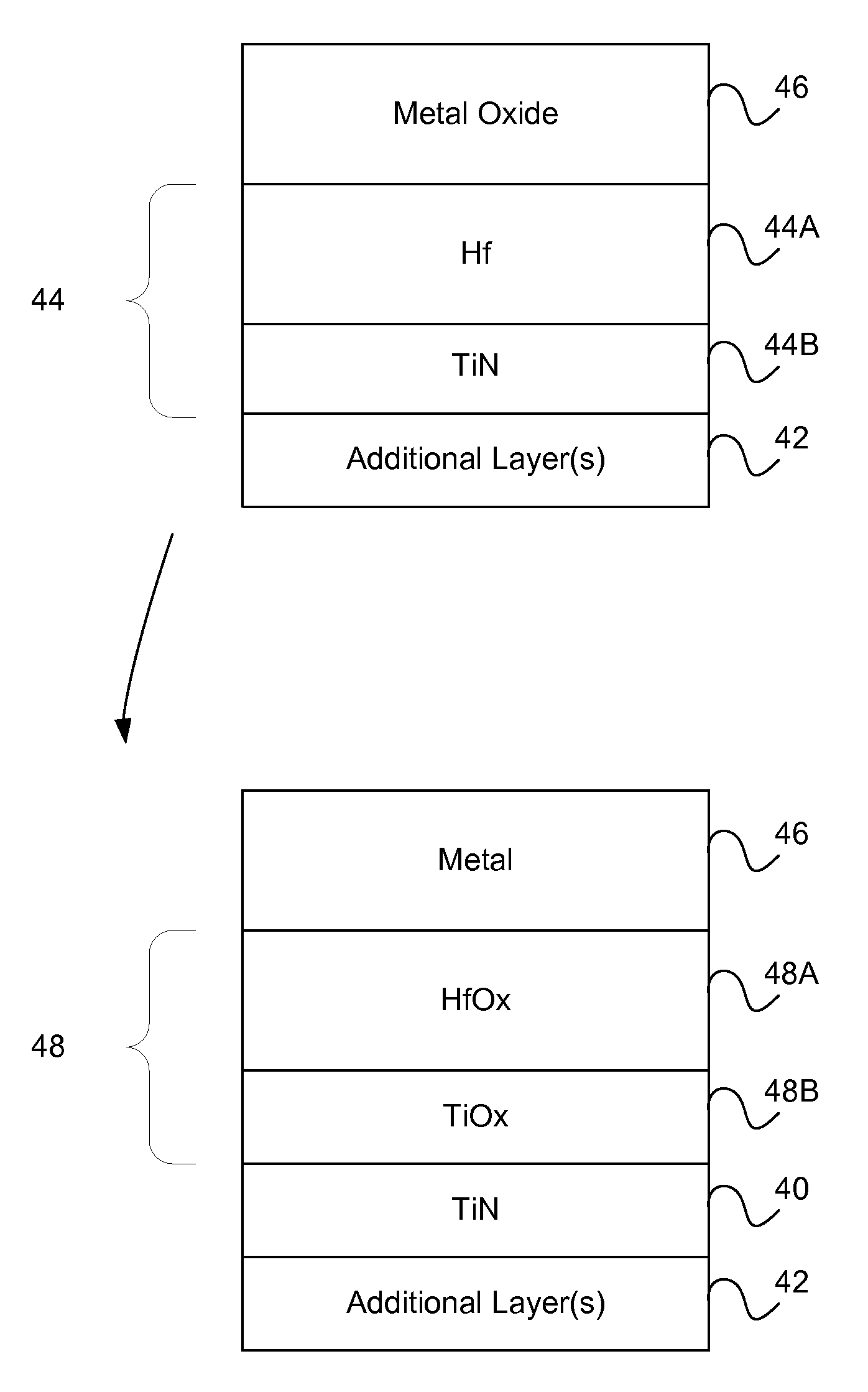
Resistive switching nonvolatile memory elements are provided. A metal-containing layer and an oxide layer for a memory element can be heated using rapid thermal annealing techniques. During heating, the oxide layer may decompose and react with the metal-containing layer. Oxygen from the decomposing oxide layer may form a metal oxide with metal from the metal-containing layer. The resulting metal oxide may exhibit resistive switching for the resistive switching memory elements.

Description

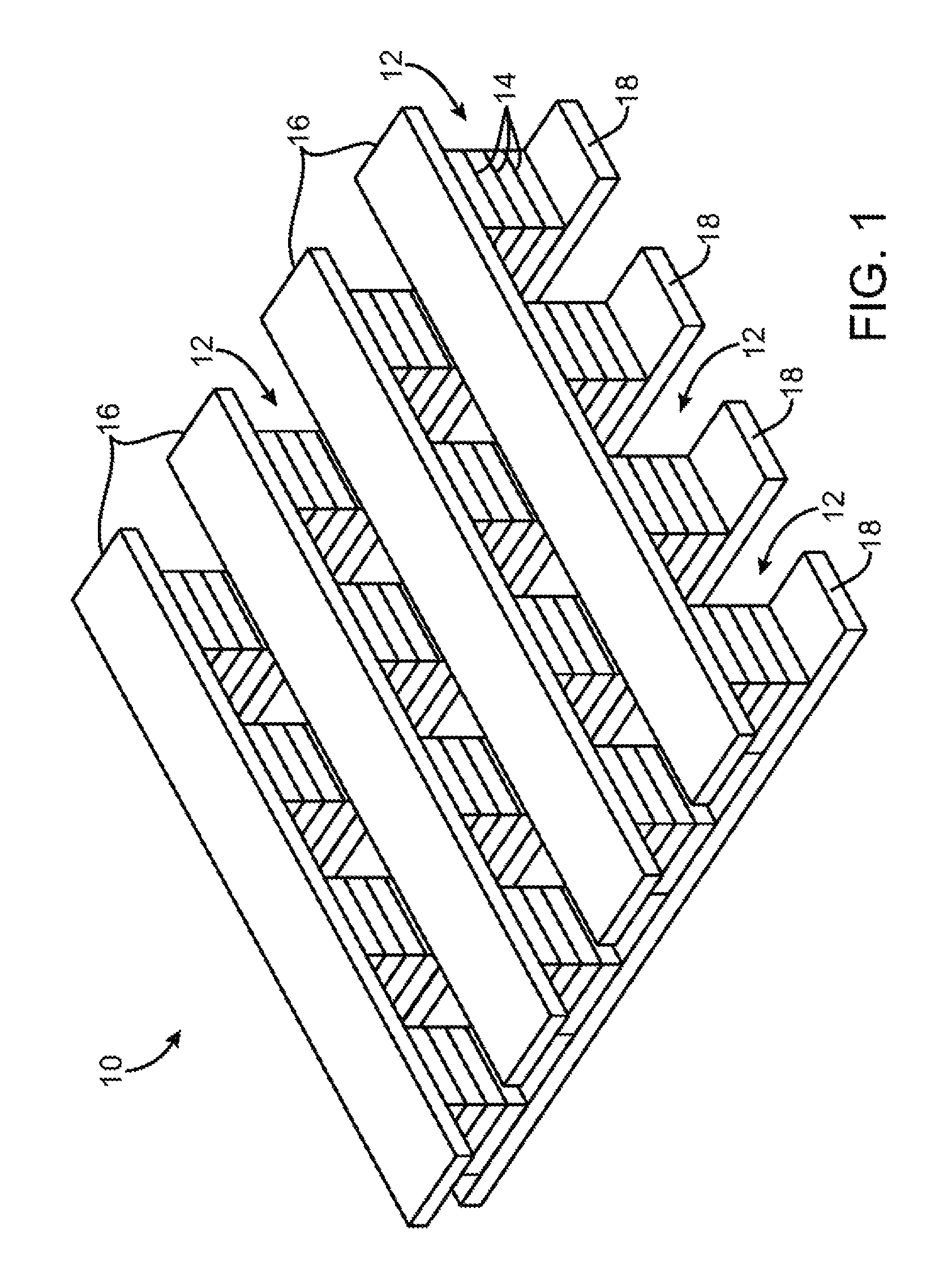
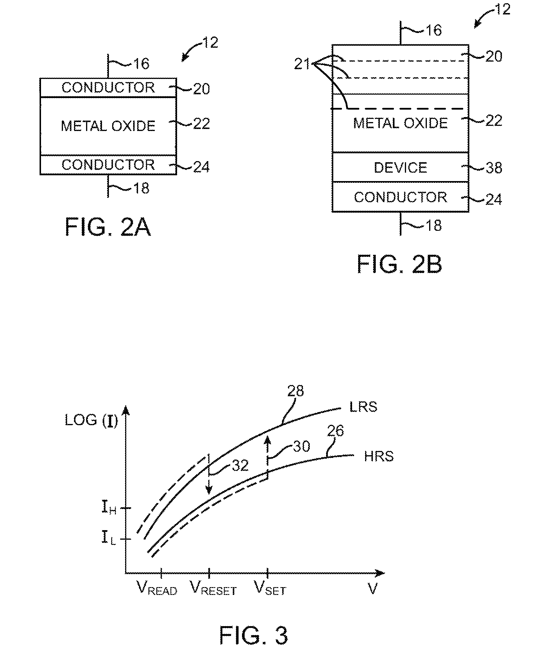
PRIORITY CLAIM TO PROVISIONAL APPLICATION[0001]A claim for priority is hereby made under the provisions of 35 U.S.C. §119 for the present application based upon U.S. Provisional Application No. 61 / 035,354 entitled “Methods for Forming Resistive Switching Memory Elements by Heating Deposited Layers” and filed on Mar. 10, 2008, which is incorporated herein by reference.FIELD OF THE INVENTION[0002]This invention relates to nonvolatile memory elements, and more particularly, to methods for forming nonvolatile resistive switching memory elements.BACKGROUND OF THE INVENTION[0003]Nonvolatile memory elements are used in systems in which persistent storage is required. For example, digital cameras use nonvolatile memory cards to store images and digital music players use nonvolatile memory to store audio data. Nonvolatile memory is also used to persistently store data in computer environments.[0004]Nonvolatile memory is often formed using electrically-erasable programmable read only memory (...

Claims


Application Information

Patent Timeline
Patent Type & Authority Patents(United States)
IPC IPC(8): H01L21/00H10N80/00
CPCH01L45/04H01L45/1233H01L45/1633H01L45/146H01L27/2463H01L27/2409H10B63/20H10B63/80H10N70/20H10N70/028H10N70/826H10N70/8833
Inventor KUMAR, PRAGATIBARSTOW, SEANSHANKER, SUNILCHIANG, TONY
Owner INTERMOLECULAR
Learn More