2-dimensional line-defects controlled silicon ingot, wafer and epitaxial wafer, and manufacturing process and apparatus therefor

a technology of epitaxial wafers and defects, applied in the direction of polycrystalline material growth, silicon compounds, under protective fluids, etc., can solve the problems of more difficult to recognize and detect defects or impurities on or in wafers, and the general detection of newly discovered defects

Active Publication Date: 2012-02-14
LG SILTRON
View PDF7 Cites 5 Cited by
  • Summary
  • Abstract
  • Description
  • Claims
  • Application Information

AI Technical Summary

Benefits of technology

[0010]Therefore, it is an object of the present invention to provide a silicon single crystalline ingot, a silicon wafer, a silicon epitaxial wafer, and a process and apparatus for manufacturing the same that reduce newly discovered crystal defects by analyzing their generation mechanism.
[0015]According to another aspect of the present invention, a process for manufacturing a silicon single crystalline ingot manufactures a silicon single crystalline ingot using the above-mentioned manufacturing apparatus, and the process includes providing the above-mentioned apparatus; preparing a silicon melt by putting silicon solid raw material in the crucible of the apparatus and heating the silicon solid raw material using a heater arranged around the crucible to melt the silicon solid raw material; and applying a horizontal magnetic field to the silicon melt received in the crucible and pulling up a silicon single crystalline ingot from the silicon melt using a silicon single crystalline seed, whereby the process controls a screw dislocation that may be generated in the silicon single crystalline ingot due to a HMCZ method.
[0021]And, the present invention may add carbon, nitrogen or oxygen as an impurity to the silicon melt to prevent propagation of a screw dislocation that may be generated in the silicon single crystalline ingot due to a HMCZ method. At this time, carbon, nitrogen or oxygen is added with a concentration of 5E14˜2E16, 5E13˜3E14 or 1E17˜1E18 atoms / cc, respectively.
[0023]According to yet another aspect of the present invention, a silicon single crystalline ingot is manufactured using the above-mentioned manufacturing apparatus, and thus is substantially free of a cross slip dislocation caused by a screw dislocation resulted from a HMCZ method.

Problems solved by technology

However, in the process for growing a silicon single crystalline ingot, crystal defects caused by crystal growing and undesired impurities that are not caused by crystal growing may be included in a silicon single crystalline ingot and a wafer.
Meanwhile, these crystal defects range from atomic level to molecular level, and their crystallographic structures are difficult to recognize and detect.
And, considering impurities not caused by crystal growing, it is more difficult to recognize and detect defects or impurities on or in a wafer.
And, newly discovered defects are generally detected when a completed wafer is inspected or a semiconductor device is formed on a wafer and inspected.
In particular, as a wafer moves toward larger diameter and a required quality level becomes higher, defects that were not regarded as a problem or detected in the past are regarded as a problem or discovered.
If such defects have not been reported so far, they are named and reported through extremely difficult study and analysis of their cause and generation mechanism.

Method used


Image

  • 2-dimensional line-defects controlled silicon ingot, wafer and epitaxial wafer, and manufacturing process and apparatus therefor
  • 2-dimensional line-defects controlled silicon ingot, wafer and epitaxial wafer, and manufacturing process and apparatus therefor
  • 2-dimensional line-defects controlled silicon ingot, wafer and epitaxial wafer, and manufacturing process and apparatus therefor

Examples


Embodiment Construction

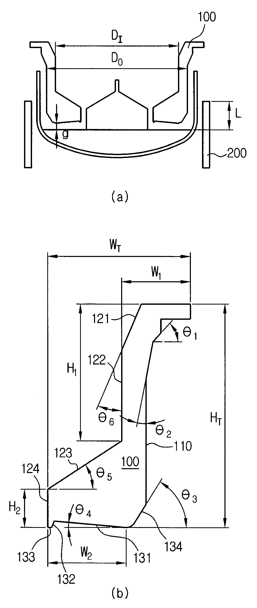
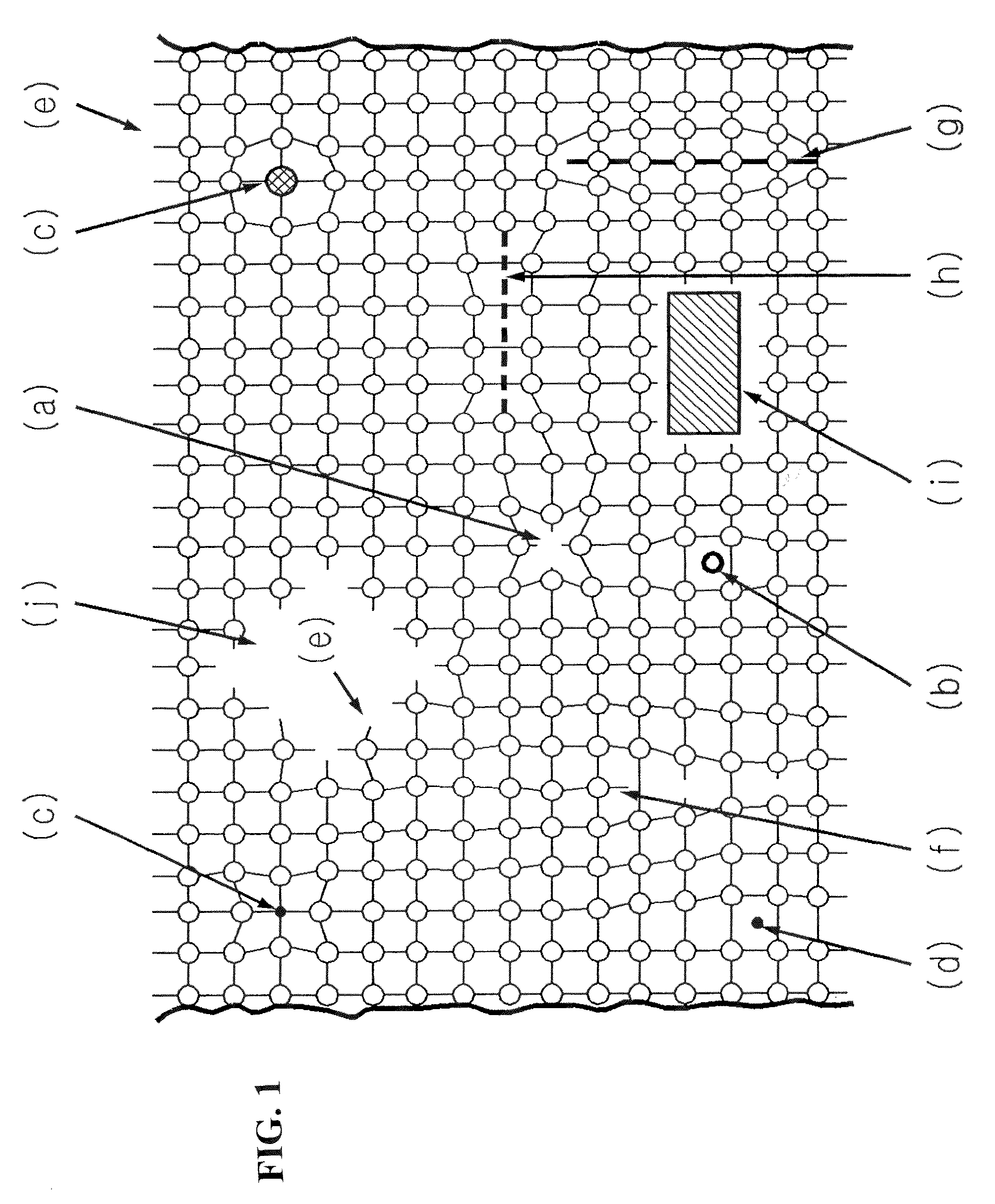
[0047]Hereinafter, new defects in a silicon single crystal discovered by the inventors of the present invention and the present invention for reducing the defects will be described in detail with reference to the accompanying drawings.

[0048]Prior to the description, it should be understood that the terms used in the specification and the appended claims should not be construed as limited to general and dictionary meanings, but interpreted based on the meanings and concepts corresponding to technical aspects of the present invention on the basis of the principle that the inventor is allowed to define terms appropriately for the best explanation. Therefore, the description proposed herein is just a preferable example for the purpose of illustrations only, not intended to limit the scope of the invention, so it should be understood that other equivalents and modifications could be made thereto without departing from the spirit and scope of the invention.

[0049]First, defects in a silico...


PUM

PropertyMeasurementUnit
angleaaaaaaaaaa
widthaaaaaaaaaa
widthaaaaaaaaaa

Abstract

The present invention reports a defect that has not been reported, and discloses a defect-controlled silicon ingot, a defect-controlled wafer, and a process and apparatus for manufacturing the same. The new defect is a crystal defect generated when a screw dislocation caused by a HMCZ (Horizontal Magnetic Czochralski) method applying a strong horizontal magnetic field develops into a jogged screw dislocation and propagates to form a cross slip during thermal process wherein a crystal is cooled. The present invention changes the shape and structure of an upper heat shield structure arranged between a heater and an ingot above a silicon melt, and controls initial conditions or operation conditions of a silicon single crystalline ingot growth process to reduce a screw dislocation caused by a strong horizontal magnetic field and prevent the screw dislocation from propagating into a cross slip.

Description

FIELD OF THE INVENTION[0001]The present invention relates to a silicon ingot, a wafer and an epitaxial wafer, and a process and apparatus for manufacturing the same, and in particular, to a technique for controlling and reducing crystal defects.BACKGROUND OF THE INVENTION[0002]In general, silicon wafers are fabricated through a process for growing a silicon single crystalline ingot, a process for slicing the ingot into disc-type wafers and a process for polishing the wafer surface, and the resultant silicon wafers are provided to manufacture semiconductor devices. However, in the process for growing a silicon single crystalline ingot, crystal defects caused by crystal growing and undesired impurities that are not caused by crystal growing may be included in a silicon single crystalline ingot and a wafer. Such crystal defects or impurities cause faults to a semiconductor device, and thus they should be removed.[0003]FIG. 1 is a view showing crystal defects reported so far. In FIG. 1,...

Claims


Application Information

Patent Timeline
Patent Type & Authority Patents(United States)
IPC IPC(8): C30B15/14C30B35/00C30B30/04C30B28/10C30B27/02C30B21/06C30B15/00C30B11/00
CPCC30B15/305C30B29/06C30B30/04C30B35/00Y10T117/1068Y10T117/1024Y10T117/10C30B15/10C30B15/20
Inventor SONG, DO-WONKIM, YOUNG-HUNJI, EUN-SANGCHOI, YOUNG-KYUJO, HWA-JIN
Owner LG SILTRON
Why Eureka
Try Eureka