
Method for producing stacked and self-aligned components on a substrate

a technology of self-alignment and substrate, which is applied in the direction of basic electric elements, semiconductor/solid-state device manufacturing, electric devices, etc., can solve the problems of high thermal budget, complex methods, and high cos

Active Publication Date: 2012-02-07
COMMISSARIAT A LENERGIE ATOMIQUE ET AUX ENERGIES ALTERNATIVES
View PDF11 Cites 2 Cited by
  • Summary
  • Abstract
  • Description
  • Claims
  • Application Information

AI Technical Summary

Benefits of technology

This method enables the efficient production of self-aligned, electrically isolated stacked components with reduced thermal budget, eliminating the need for costly lithography and complex processes, while maintaining high selectivity and precision in component formation.

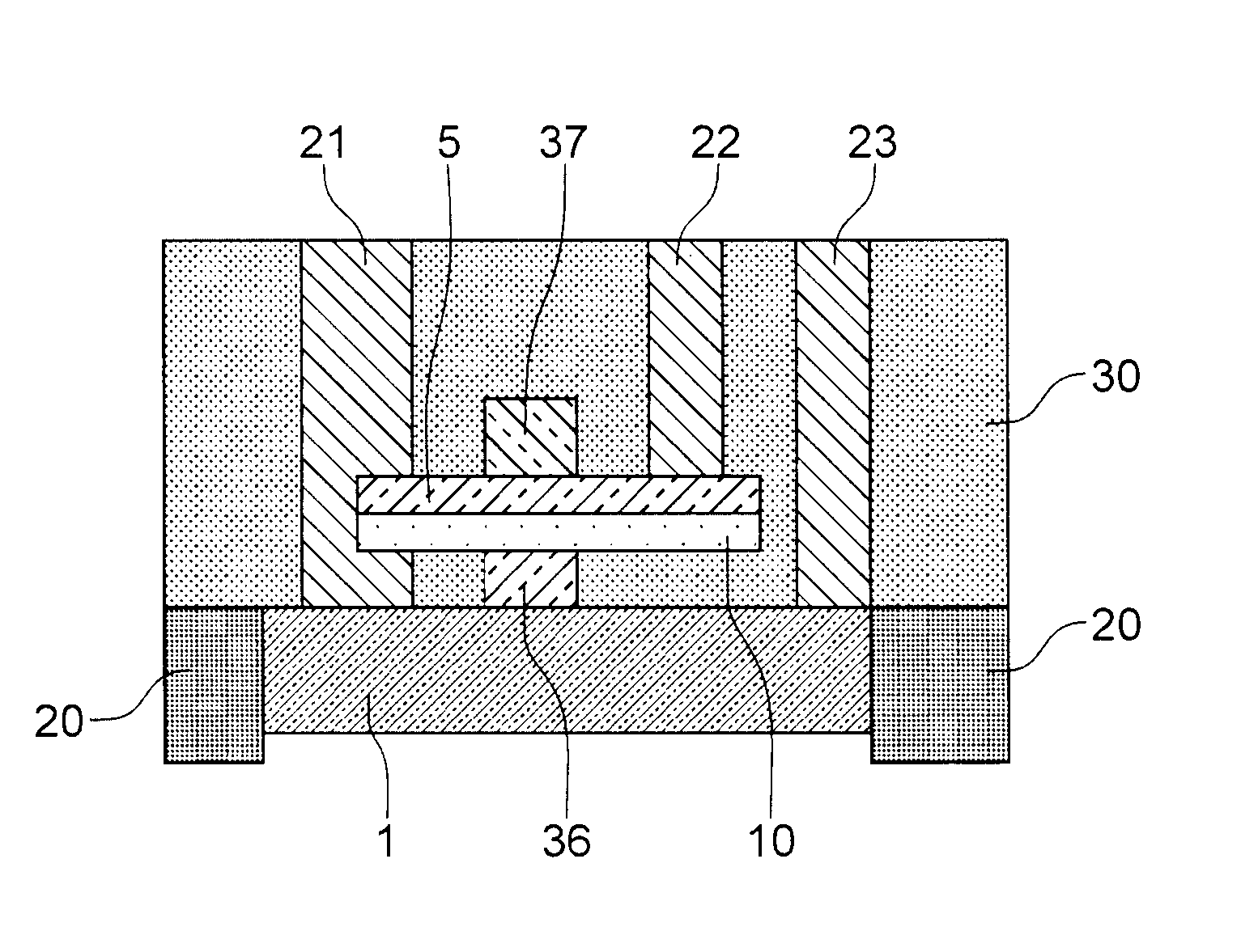
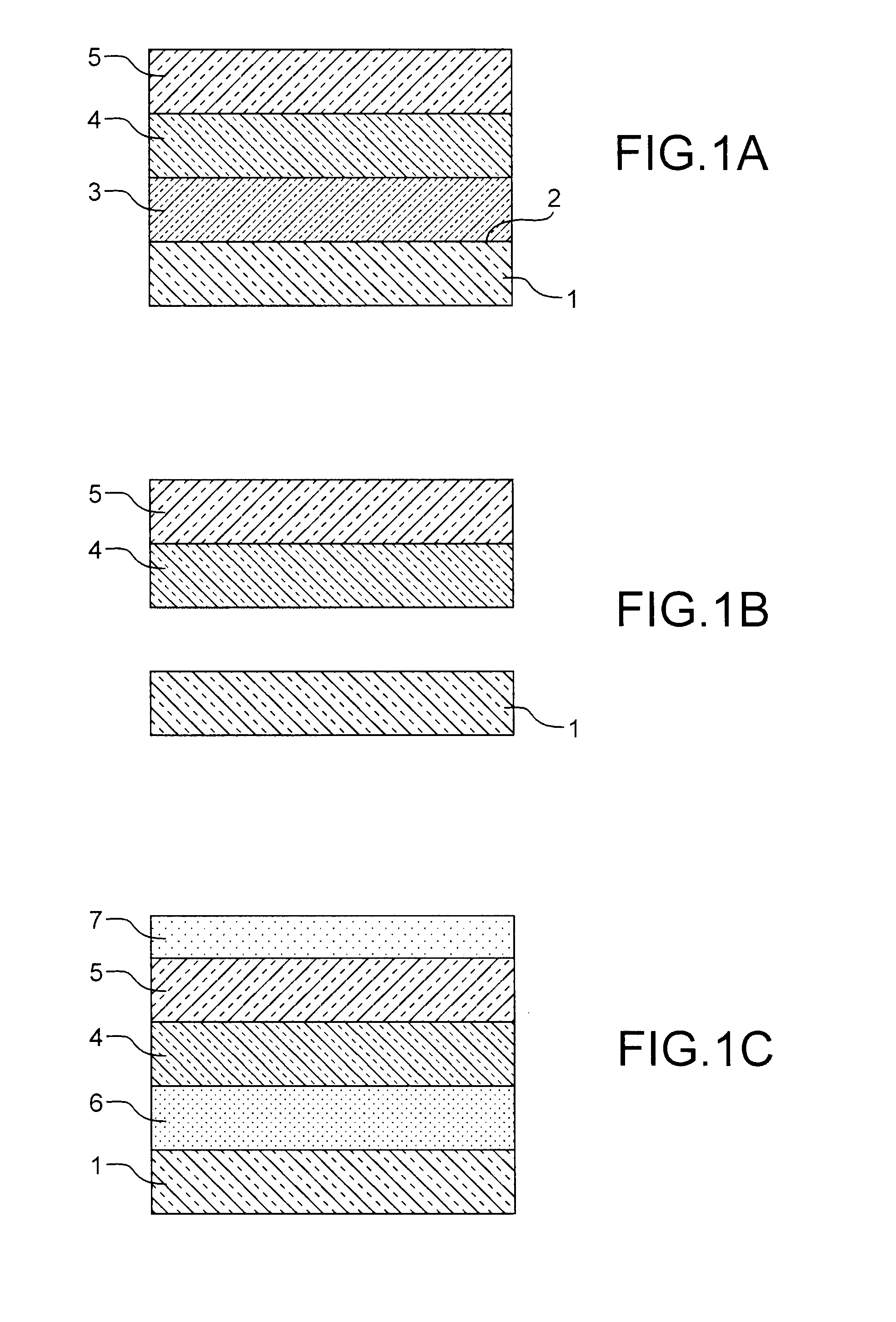
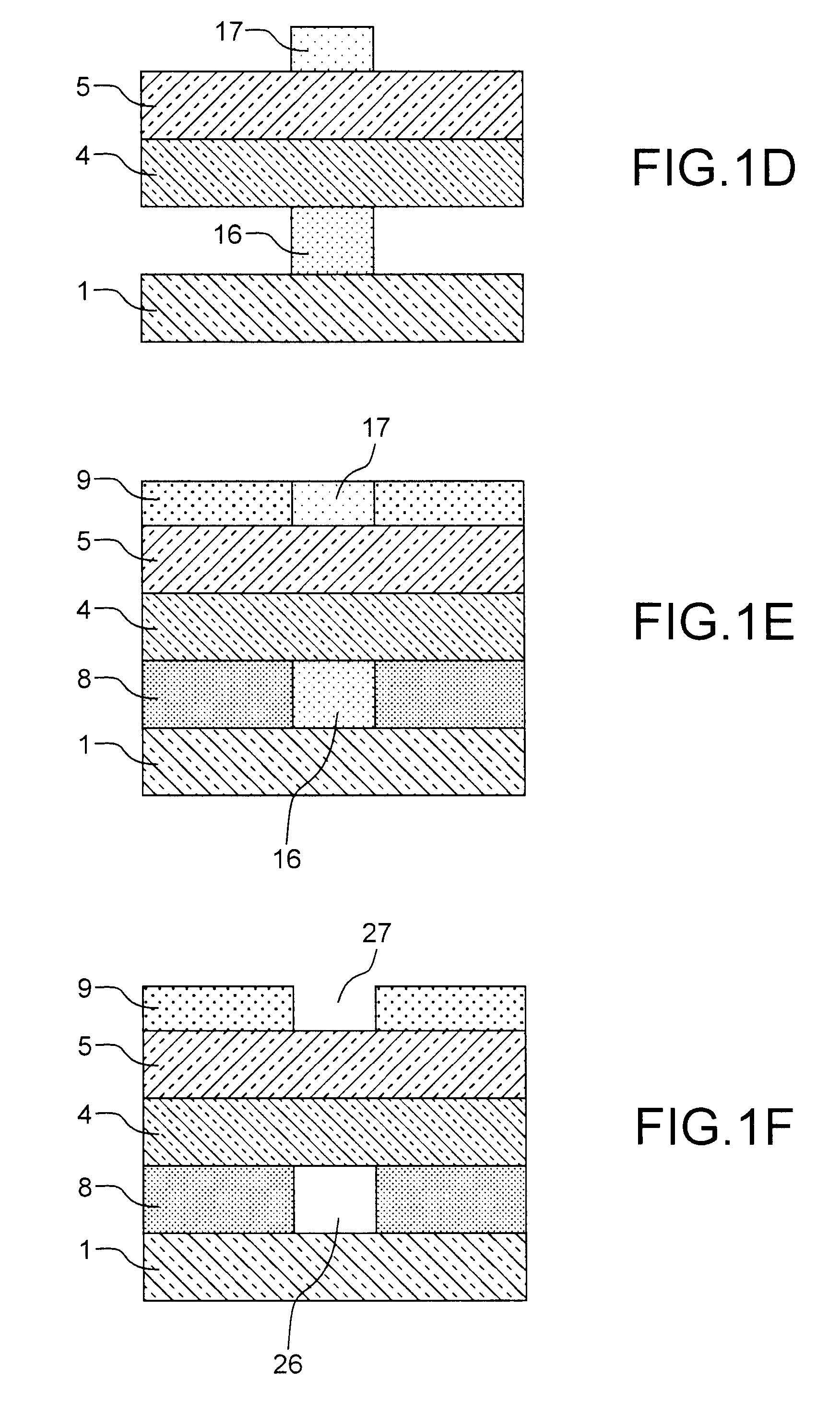
Problems solved by technology

This concept however often draws upon methods that are complex, high in thermal budget and / or costly (re-crystallisation of silicon, molecular bonding, re-growth through a contact, numerous lithographies, etc.).

Method used


Image

  • Method for producing stacked and self-aligned components on a substrate
  • Method for producing stacked and self-aligned components on a substrate
  • Method for producing stacked and self-aligned components on a substrate

Examples


Embodiment Construction

[0013]As described previously, the formation of self-aligned stacked functions necessitates the use of high thermal budget methods (re-crystallisation of silicon through contact holes), complex methods (laser assisted epitaxial growth) or expensive methods (use of several sets of lithography masks).

[0014]The present invention describes a method for stacking, on several levels (at least two), components that are self-aligned and electrically isolated from each other (semiconductors, microresonators, etc.) by an insulator layer. No method of recrystallisation of silicon, regrowth through a contact is necessary, thereby limiting the thermal budget constraints. The stacks are defined as of the first operation by epitaxy. Selective etchings and the use of self-aligned lithography then make it possible to work through the membrane.

[0015]The object of the invention is a method for producing stacked and self-aligned components on a substrate, comprising the following steps:

[0016]providing a...


PUM

PropertyMeasurementUnit
temperatureaaaaaaaaaa

Abstract

A method for producing stacked and self-aligned components on a substrate, including: providing a substrate made of monocrystalline silicon having one face enabling production of components, forming a stack of layers on the face of the substrate, selective etching by a gaseous mixture comprising gaseous HCl conveyed by a carrier gas and at a temperature between 450° C. and 900° C., depositing resin, implementing lithography of the resin, replacing resin eliminated during the lithography with a material for confining remaining resin, and forming elements of the components.

Description

TECHNICAL FIELD[0001]The invention relates to a method for producing stacked and self-aligned components on a substrate.[0002]It applies in particular, but not exclusively, to the formation of self-aligned stacked functions constituting electronic components or parts thereof, elements of MEMS, etc.STATE OF THE PRIOR ART[0003]The formation of components stacked one above the other has known a certain success, whether in microelectronics or in other fields (MEMS, etc.). It is even possible to stack components such as transistors and MEMS. This concept however often draws upon methods that are complex, high in thermal budget and / or costly (re-crystallisation of silicon, molecular bonding, re-growth through a contact, numerous lithographies, etc.).[0004]Among the known techniques for forming stacked functions, the following techniques may be cited.[0005]A first technique implements a repeat epitaxy through contact holes. The epitaxial growth is laser assisted. This technique has been pr...

Claims


Application Information

Patent Timeline
Patent Type & Authority Patents(United States)
IPC IPC(8): H01L21/8238
CPCH01L21/76264H01L21/8221H01L21/84
Inventor WACQUEZ, ROMAINCORONEL, PHILIPPEDESTEFANIS, VINCENTHARTMANN, JEAN-MICHEL
Owner COMMISSARIAT A LENERGIE ATOMIQUE ET AUX ENERGIES ALTERNATIVES
Learn More