Semiconductor device package with internal device protection

a technology of internal device protection and semiconductor devices, which is applied in the direction of semiconductor/solid-state device details, fixed capacitor details, fixed capacitors, etc., can solve the problems of system and circuit design using those parts, user might even be very reluctant to use, and change the system circuitry

Inactive Publication Date: 2012-01-24
INFINEON TECH AMERICAS CORP
View PDF23 Cites 6 Cited by
  • Summary
  • Abstract
  • Description
  • Claims
  • Application Information

AI Technical Summary

Benefits of technology

[0015]The invention provides a solution for the above described problem of replacement parts that require additional protection compared to the replaced predecessor device. In accordance with the invention, a protecting pre-resistor or other device is integrated into the standard package of the new device without impact on footprint and pin compatibility. For example, a resistor, which may have a well controlled thermal coefficient of resistance may be added to the lead frame pine of the device. The package will then provide the protection needs of the new device without requiring the customer to redesign his circuit to accommodate the new part.
[0018]b) Cost and space savings as compared to the state of the art solution that requires an additional external passive component (like a pre-resistor) in the circuitry to protect the new replacement part.
[0019]c) Quick adoption of newer generation parts without cost and time intensive redesigns at the customer site.

Problems solved by technology

On the other hand this quick replacement of existing parts by newer devices can also cause many problems for the system and circuit designs using those parts.
Unfortunately, even if pin-compatibility can be achieved, newer silicon or GaN technology might have different electric characteristics that require changes of the system circuitry even if the package outline and the footprint of the replacement part are identical to the predecessor package.
In some cases a user might even be very reluctant to use it due to the need for additional changes in his system circuitry.
This is a major drawback for the quick adaptation of replacement parts with newer silicon or other technology and better performance.
a) the user has to implement the changes on his system and carry the cost and time delay for changing the entire system such as a different PCB layout and changes in the assembly process to implement the pre-resistor or other component.
b) if the user is not aware of the need for a pre-resistor he might just replace the older generation part with the newer “pin-compatible” product and cause unaccepted failures in his application.

Method used


Image

  • Semiconductor device package with internal device protection
  • Semiconductor device package with internal device protection
  • Semiconductor device package with internal device protection

Examples


Embodiment Construction

[0036]Referring now to the drawings, similar components in each Figure have the same identifying numeral.

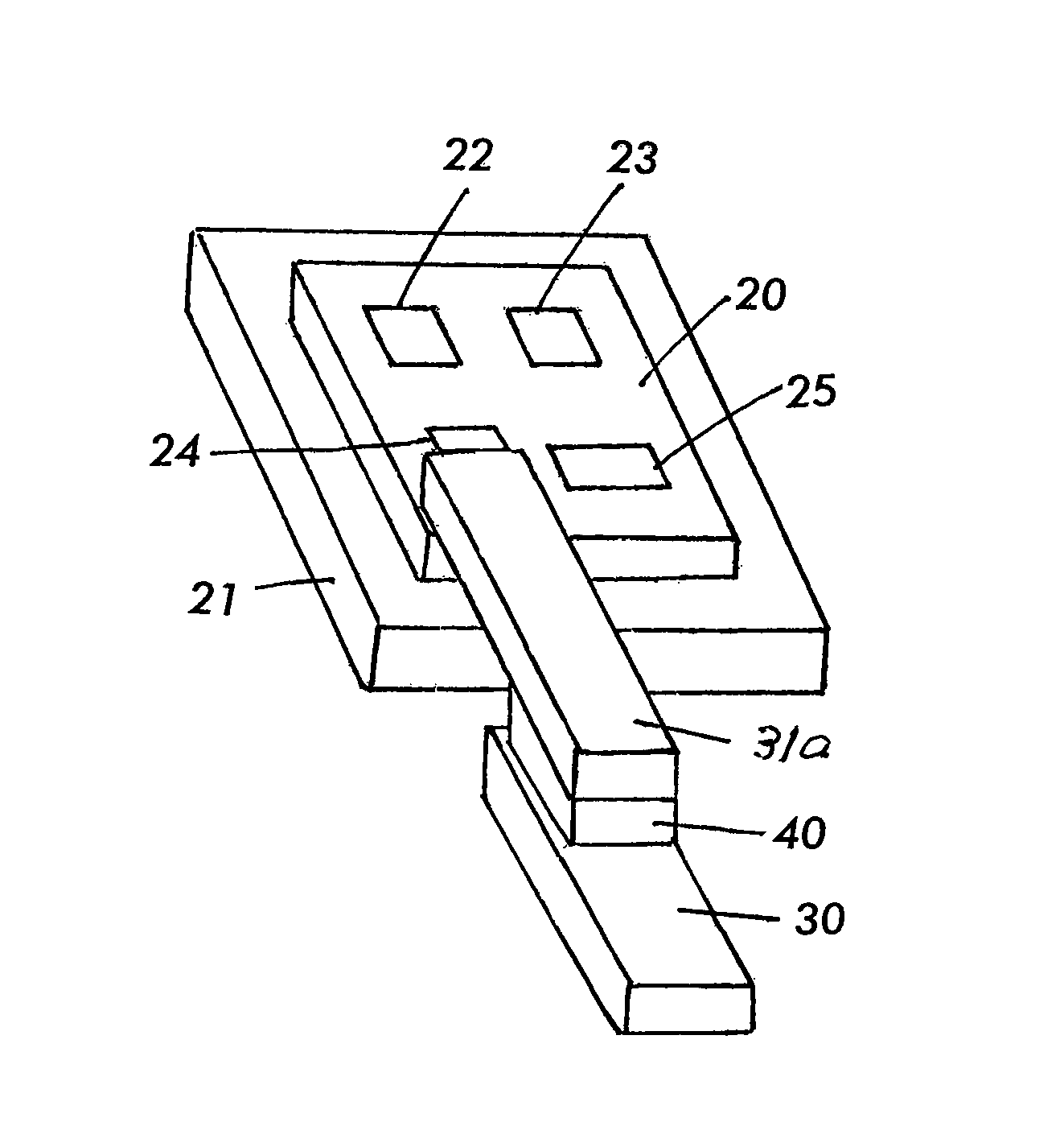
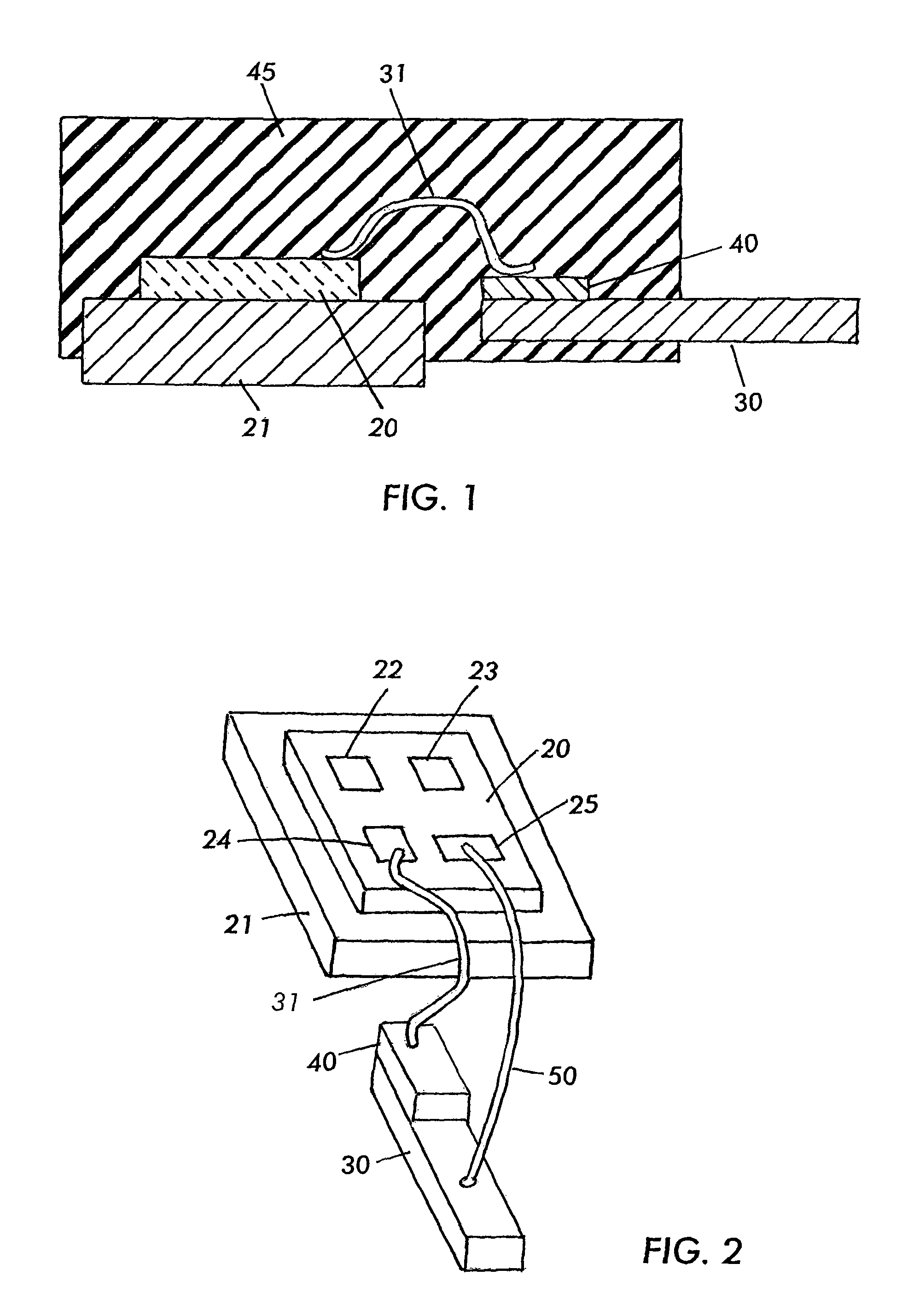
[0037]Referring first to FIG. 1, there is shown a processed silicon die 20 mounted on a lead frame segment 21.

[0038]Die 20 may be an IC or power device such as a MOSFET or IGBT or the like and may include process improvements over the processes used for part which it replaces. The die 20 may have any desired electrode pattern, including for example, electrodes 22, 23, 24 and 25 (FIGS. 2, 3, 5 and 6) depending on the device 20 type.

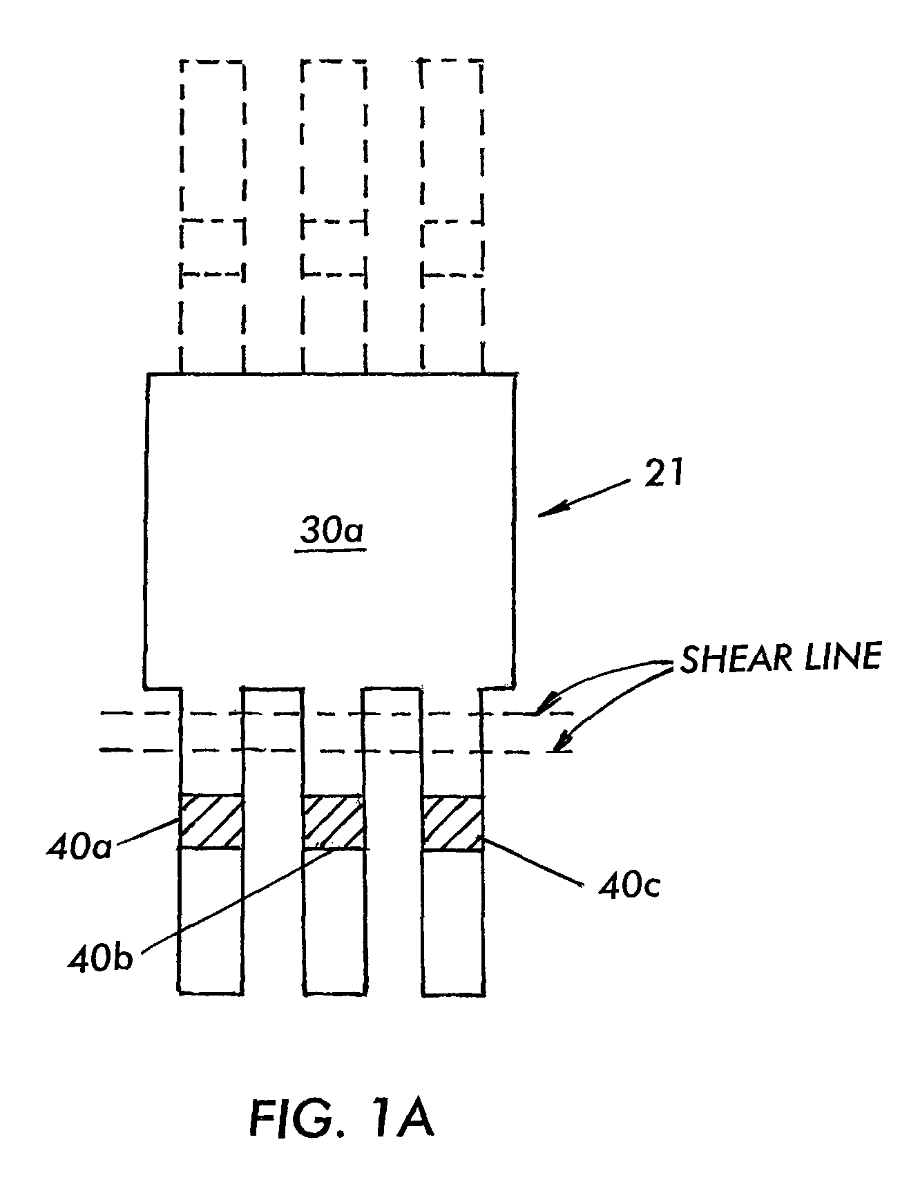
[0039]Lead frame 21 (FIGS. 1, 2, 3, 4, 5 and 6) has a plurality of extending leads or pins, only one of which, lead 30, is shown in FIG. 1. A conventional wire bond 31 bonds electrode 24 to lead 30. Other wire bonds may connect the other electrodes to other lead frame leads or pins (not shown).

[0040]In accordance with one embodiment of the invention, and as shown in FIG. 1, a pre-resistor 40 is fixed on lead frame lead 30 and receives the end of bond wi...


PUM


Abstract

An integral impedence is formed on or within a lead frame pin of a semiconductor package and receives a connection from an electrode of a semiconductor die within the package to eliminate the need for adjustment and protective impedences external of the package. The impedence comprises passives such as resistors, capacitors, diodes or inductors which modify the performance of the package for new semiconductor device characteristics. The impedences may have positive or negative temperature coefficients and are in close thermal communication with the semiconductor die.

Description

BACKGROUND OF THE INVENTION[0001]Modern applications of semiconductor packages have an increasing demand for quick improvements in performance of their electric components and circuits. To keep up with the raising demand of better performance, higher power density, more efficiency, lower cost and space, more integration, higher functionality, increased digital content, etc., the silicon process technologies undergo continuous improvement steps. Correspondingly the technology development cycles of entire silicon process platforms have shrunk dramatically, sometimes with intermediate process upgrades on a yearly time base.[0002]Consequently the market and the applications can take advantage of newer and better performing devices on shorter and shorter time scales. Existing products will be replaced by a next generation part with faster turn-around cycles than ever before. The quick adoption of a better performing silicon (or other semiconductor materials) process technology is advanta...

Claims


Application Information

Patent Timeline
Patent Type & Authority Patents(United States)
IPC IPC(8): H05K7/10
CPCH01L23/495H01L23/4952H01L23/49541H01L23/49589H01L24/06H01L24/48H01L24/49H01L23/3107H01L24/45H01L2224/04042H01L2224/05553H01L2224/05647H01L2224/45124H01L2224/45144H01L2224/48091H01L2224/48247H01L2224/48472H01L2224/49113H01L2224/85447H01L2924/01002H01L2924/01005H01L2924/01013H01L2924/01014H01L2924/01025H01L2924/01027H01L2924/01028H01L2924/01029H01L2924/01042H01L2924/01075H01L2924/01078H01L2924/01079H01L2924/01082H01L2924/014H01L2924/13055H01L2924/13091H01L2924/19041H01L2924/19042H01L2924/19043H01L2924/3011H01L2924/00014H01L2924/01006H01L2924/01033H01L2924/00H01L2224/48647H01L2224/48747H01L2224/49109H01L2924/10253H01L2924/181H01L2924/00012
Inventor HAUENSTEIN, HENNING M.NAKATA, ALANA
Owner INFINEON TECH AMERICAS CORP
Why Eureka
Try Eureka