
Double data rate (DDR) counter, analog-to-digital converter (ADC) using the same, CMOS image sensor using the same and methods in DDR counter, ADC and CMOS image sensor

a counter and data rate technology, applied in the field of image sensors and analog-to-digital converters (adcs) and counters for image sensors, can solve the problems of frequent toggling of the least significant bit (lsb), high-speed counters, ripple counters,

Active Publication Date: 2011-08-02
SAMSUNG ELECTRONICS CO LTD
View PDF21 Cites 34 Cited by
  • Summary
  • Abstract
  • Description
  • Claims
  • Application Information

AI Technical Summary

Benefits of technology

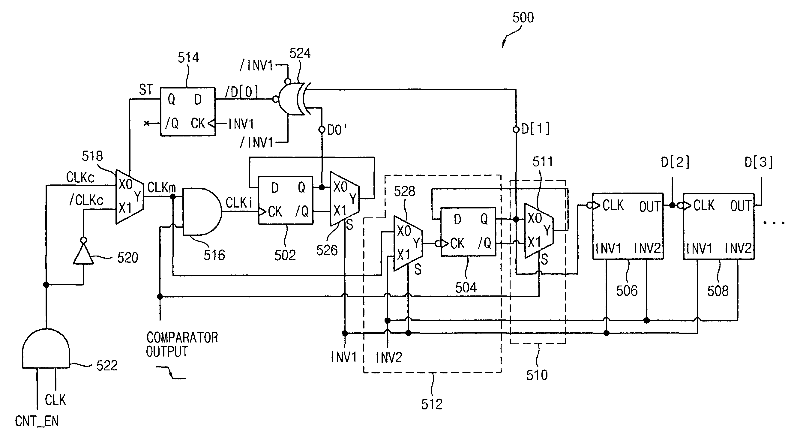
The patent describes a double data rate (DDR) counter that generates a least significant bit (LSB) of a plurality of bits based on an input signal. The counter includes a first stage that is triggered on either a rising or falling edge of the input signal and a second stage that is triggered on the other of the rising or falling edge. The counter can be used in an analog-to-digital converter (ADC) for correlated double sampling. The technical effect of the invention is to provide a more efficient and accurate method for generating the LSB of a plurality of bits in an ADC.

Problems solved by technology

High-speed counters, such as ripple counters, used in CDS consume a large amount of power.
One particular cause of the power consumption in such counters is the frequent toggling of the least significant bit (LSB) in the counter.

Method used


Image

  • Double data rate (DDR) counter, analog-to-digital converter (ADC) using the same, CMOS image sensor using the same and methods in DDR counter, ADC and CMOS image sensor
  • Double data rate (DDR) counter, analog-to-digital converter (ADC) using the same, CMOS image sensor using the same and methods in DDR counter, ADC and CMOS image sensor
  • Double data rate (DDR) counter, analog-to-digital converter (ADC) using the same, CMOS image sensor using the same and methods in DDR counter, ADC and CMOS image sensor

Examples


Embodiment Construction

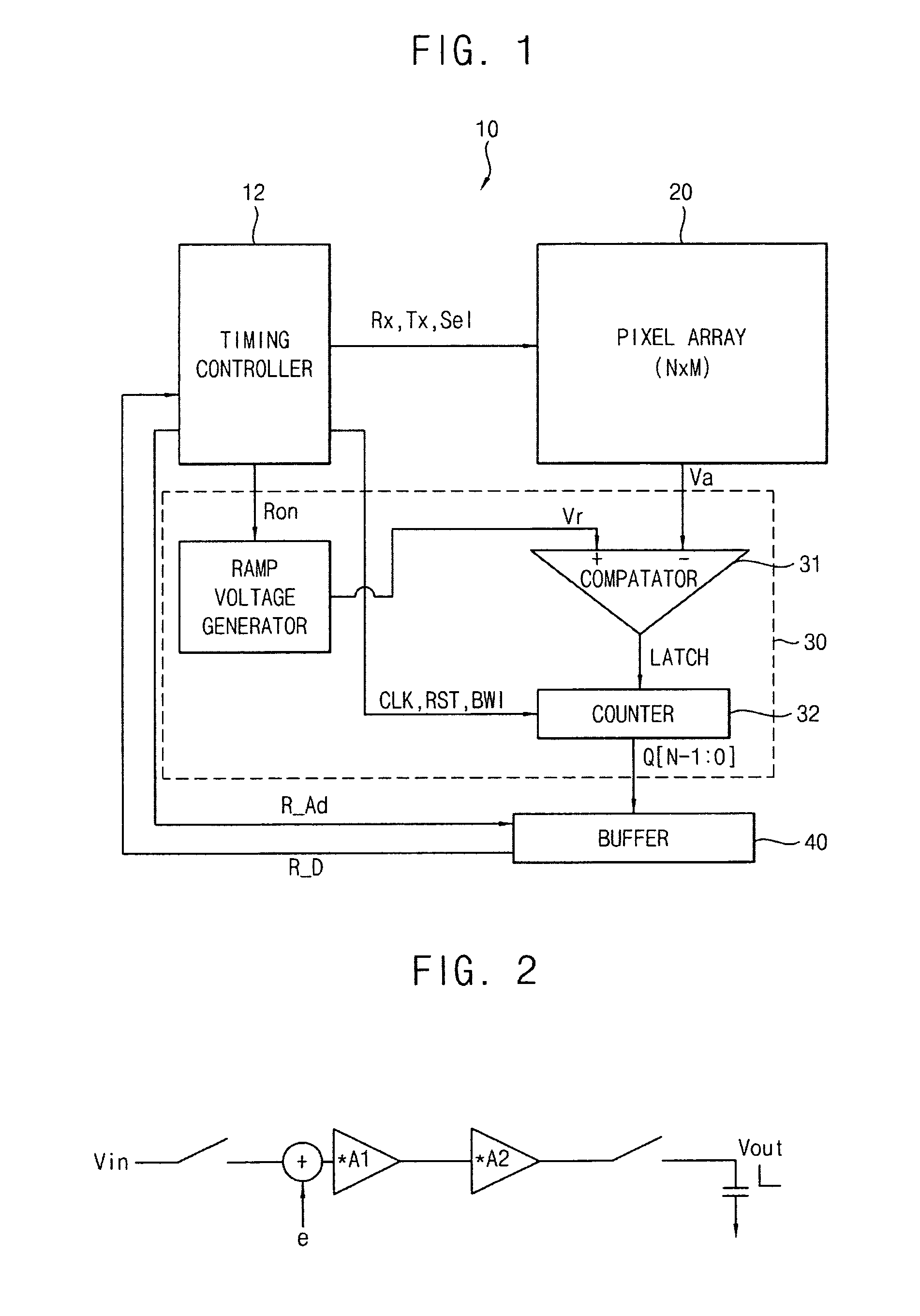
[0093]FIG. 1 includes a schematic block diagram of a general CMOS image sensor (CIS) 10. The CIS 10 may be used, for example, in a digital still camera. Referring to FIG. 1, the CIS 10, which converts external image data into digital data and stores the digital data, includes a timing controller 12, an active pixel sensor array (APS), or, simply, a pixel array 20, an analog-to-digital converter (ADC) 30, and a buffer 40.

[0094]The pixel array 20 receives external image data, i.e., from outside the CMOS image sensor 10, and outputs an analog signal Va to ADC 30 in response to control signals Rx, Tx and Sel received from the timing controller 12. The analog signal Va may also be referred to as a “pixel signal” or “data signal” or “image signal” or “input signal” or the like. The ADC 30 includes a comparator 31, a counter 32 and a ramp voltage generator 33. The comparator 31 receives the analog signal Va and receives a ramp signal Vr from ramp voltage generator 33. A “ramp signal” is a ...


PUM


Abstract

In a double data rate (DDR) counter and counting method used in, for example, an analog-to-digital conversion in, for example, a CMOS image sensor and method, a first stage of the counter generates a least significant bit (LSB) of the value in the counter. The first stage includes a first clock input and is edge-triggered on one of the rising and falling edges of a signal applied at the first clock input. The counter includes at least one second stage for generating another bit of the value in the counter. The second stage includes a second clock input and is edge-triggered on the other of the rising and falling edges of a signal applied at the second clock input.

Description

RELATED APPLICATION[0001]This application relies for priority under 35 U.S.C. 119(a) on Korean Patent Application number 10-2009-0011692, filed in the Korean Intellectual Property Office on Feb. 13, 2009, the entire contents of which are incorporated herein by reference.BACKGROUND[0002]1. Field of the Invention[0003]This application relates to image sensors and analog-to-digital converters (ADCs) and counters for image sensors and, more particularly, to a counter and an ADC and methods in a CMOS image sensor.[0004]2. Description of the Related Art[0005]Complementary metal-oxide-semiconductor (CMOS) image sensors (CISs), which are widely used in digital cameras, capture optical signals and convert the optical signals into electrical signals. The CMOS image sensor has an active pixel sensor (APS) array that includes multiple pixels arranged in rows and columns. Each pixel typically includes a photodiode and a processing or read-out circuit. The photodiode generates electrical charge u...

Claims


Application Information

Patent Timeline
Patent Type & Authority Patents(United States)
IPC IPC(8): H03M1/34
CPCH03K21/023H03K21/38H03K23/548
Inventor LIM, YONGKOH, KYOUNG-MINKIM, KYUNG-MIN
Owner SAMSUNG ELECTRONICS CO LTD
Learn More