
Method and system for step-and-align interference lithography

a technology of interference lithography and step-and-aligning, which is applied in the field of interference lithography (il) technology, can solve the problems of insufficient precision for manufacturing microstructures whose critical mobile platform of piezoelectric actuators is only capable of traveling in a very short stroke, and achieves high precision

Inactive Publication Date: 2011-06-28
IND TECH RES INST
View PDF2 Cites 5 Cited by
  • Summary
  • Abstract
  • Description
  • Claims
  • Application Information

AI Technical Summary

Benefits of technology

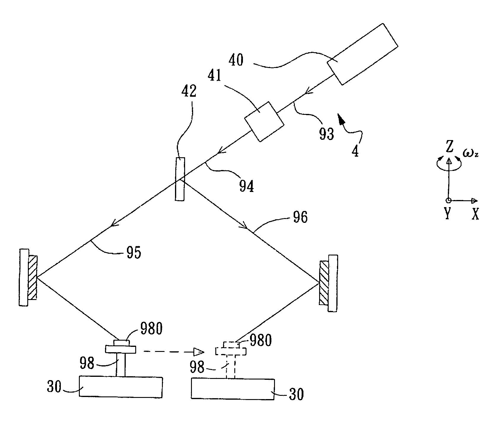
The present invention provides a method and system for step-and-align interference lithography, which allows for accurate alignment of interference-patterned regions on a two-dimensional plane for stitching together in high precision. The method includes steps of measuring displacement error of interference light beams caused by moving the carrier or light beams in a stepwise manner, and then using the displacement error as a reference to compensate positioning errors between adjacent interference patterns during step-and-align interference lithography. The system includes a carrier, position detecting unit, stage driving unit, interference lithography unit, and signal processing unit. The technical effects of the invention include accurate alignment of interference-patterned regions and high precision in stitching together multiple regions.

Problems solved by technology

In addition, as the positioning of the aforesaid patent is not performed by a mechanical mechanism, the platform for the aforesaid interference lithography method can enjoy a comparatively longer lifespan.
Although following the progress of motor control technique and the advance of fabrication process for mechanical parts, those long-stroke, low-precision positioning device, represented by a device composed of motors and screw rods that is designed with a stroke of about 200 mm, can achieve micron-scaled or even submicron-scaled positioning accuracy, their precisions are still not good enough for manufacturing microstructures whose critical dimensions are smaller than submicron.
However, such mobile platform of piezoelectric actuator is only capable of traveling in a very short stroke, which can be no more than 0.5 mm in general.

Method used


Image

  • Method and system for step-and-align interference lithography
  • Method and system for step-and-align interference lithography
  • Method and system for step-and-align interference lithography

Examples


Embodiment Construction

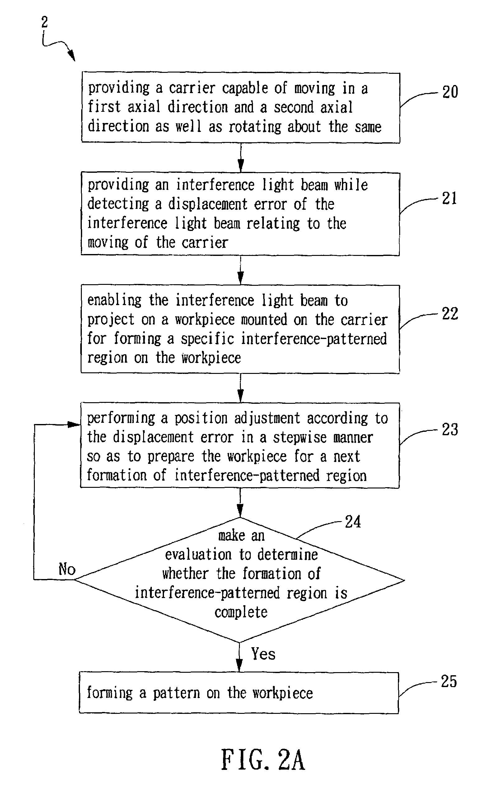
[0028]For your esteemed members of reviewing committee to further understand and recognize the fulfilled functions and structural characteristics of the invention, several exemplary embodiments cooperating with detailed description are presented as the follows. Please refer to FIG. 2A, which is a flow chart depicting the steps of a method for step-and-align interference lithography according to an exemplary embodiment of the invention. The method starts from step 20. At step 20, a carrier capable of moving in a first axial direction and a second axial direction as well as rotating about the same is provided, which is used for carrying a substrate for interference lithography whereas the substrate can be made of a silicon material, but is not limited thereby; and then the flow proceeds to step 21. At step 21, an interference light beam is provided and further g a displacement error of the interference light beam relating to the moving of the carrier is also being detected; and then t...


PUM


Abstract

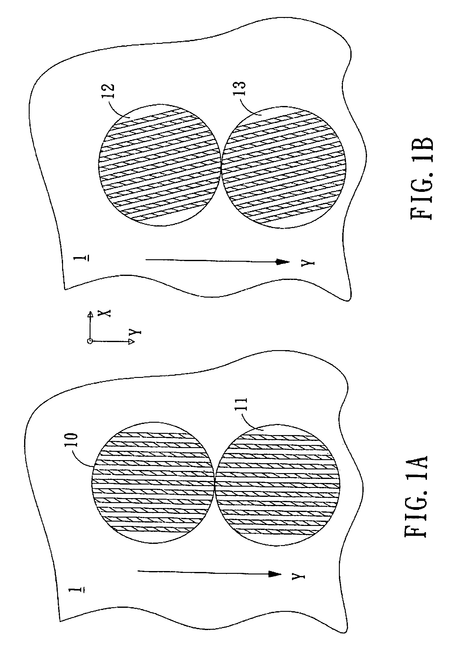
A method for step-and-align interference lithography is provided in the present invention, by which a displacement error relating to the moving of an interference light beam as the source of the interference light beam is being carried to move by a carrier is measured before interference lithography, and then the displacement error is used as a reference to compensate a positioning error between adjacent interference patterns during step-and-align interference lithography. Besides, the present invention further provides a system for step-and-align interference lithography, which is capable of compensating the positioning error caused by a stepping movement control used for moving a substrate or the light beams in a stepwise manner to form interference-patterned regions by interference lithography and thus the so-generated interference-patterned regions are accurate aligned with one another on a two-dimensional plane for preparing the same to be stitched together to form a two-dimensional large-area periodic structure.

Description

FIELD OF THE INVENTION[0001]The present invention relates to an interference lithography (IL) technology, and more particularly, to a step-and-align IL method and system with positioning error compensation ability.BACKGROUND OF THE INVENTION[0002]Recently, with the increasing demand of large-area applications in displays, flexible electronic devices and solar cells, it is required that opto-electronic devices are manufactured in large area by the composition of periodic sub-structures whose critical dimensions are preferred to be the smaller the better. It is predictable that there will be more and more manufacturers focusing their effort on submicron-scaled, or even nano-scaled periodic structures. However, to achieve such submicron-scaled, or nano-scaled periodic structures, it is important to have an alignment device capable of positioning in nano-scaled precision, which is especially true for trying to manufacture a large-area device with microstructures by a means of interferen...

Claims


Application Information

Patent Timeline
Patent Type & Authority Patents(United States)
IPC IPC(8): G01B11/02
CPCG03B27/42G03F7/70475G03F7/70408
Inventor YEN, JIA-YUSHCHANG, SHUO-HUNGCHEN, CHENG-HUNGCHEN, LIEN-SHENG
Owner IND TECH RES INST
Learn More