
Nonvolatile memory device, nonvolatile memory system, and defect management method for nonvolatile memory device

a nonvolatile memory and defect management technology, applied in measurement devices, electronic circuit testing, instruments, etc., can solve the problems of difficult manufacturing flash memory that can guarantee 10,000 times of rewriting, low guaranteed number of rewriting, etc., and achieve accurate and easy recognition of the life of the nonvolatile memory device

Active Publication Date: 2011-04-05
PANASONIC CORP
View PDF13 Cites 2 Cited by
  • Summary
  • Abstract
  • Description
  • Claims
  • Application Information

AI Technical Summary

Benefits of technology

Enables users to easily and accurately recognize when a semiconductor memory card's life is nearing expiration, facilitating timely replacement and reducing anxiety about data loss, especially in professional applications like moving image recorders.

Problems solved by technology

Such a multi-level NAND flash memory has difficulties in ensuring the reliability of a memory cell and thus has a low guaranteed number of times of rewriting.
Moreover, it also becomes difficult to manufacture a flash memory that can guarantee 10,000 times of rewriting.
However, when using a product loaded with the flash memory whose guaranteed number of times of rewriting is limited, it is important especially for users who frequently rewrite data to use it with consideration given to the life or to select a product while keeping the product life in mind.

Method used


Image

  • Nonvolatile memory device, nonvolatile memory system, and defect management method for nonvolatile memory device
  • Nonvolatile memory device, nonvolatile memory system, and defect management method for nonvolatile memory device
  • Nonvolatile memory device, nonvolatile memory system, and defect management method for nonvolatile memory device

Examples


embodiment

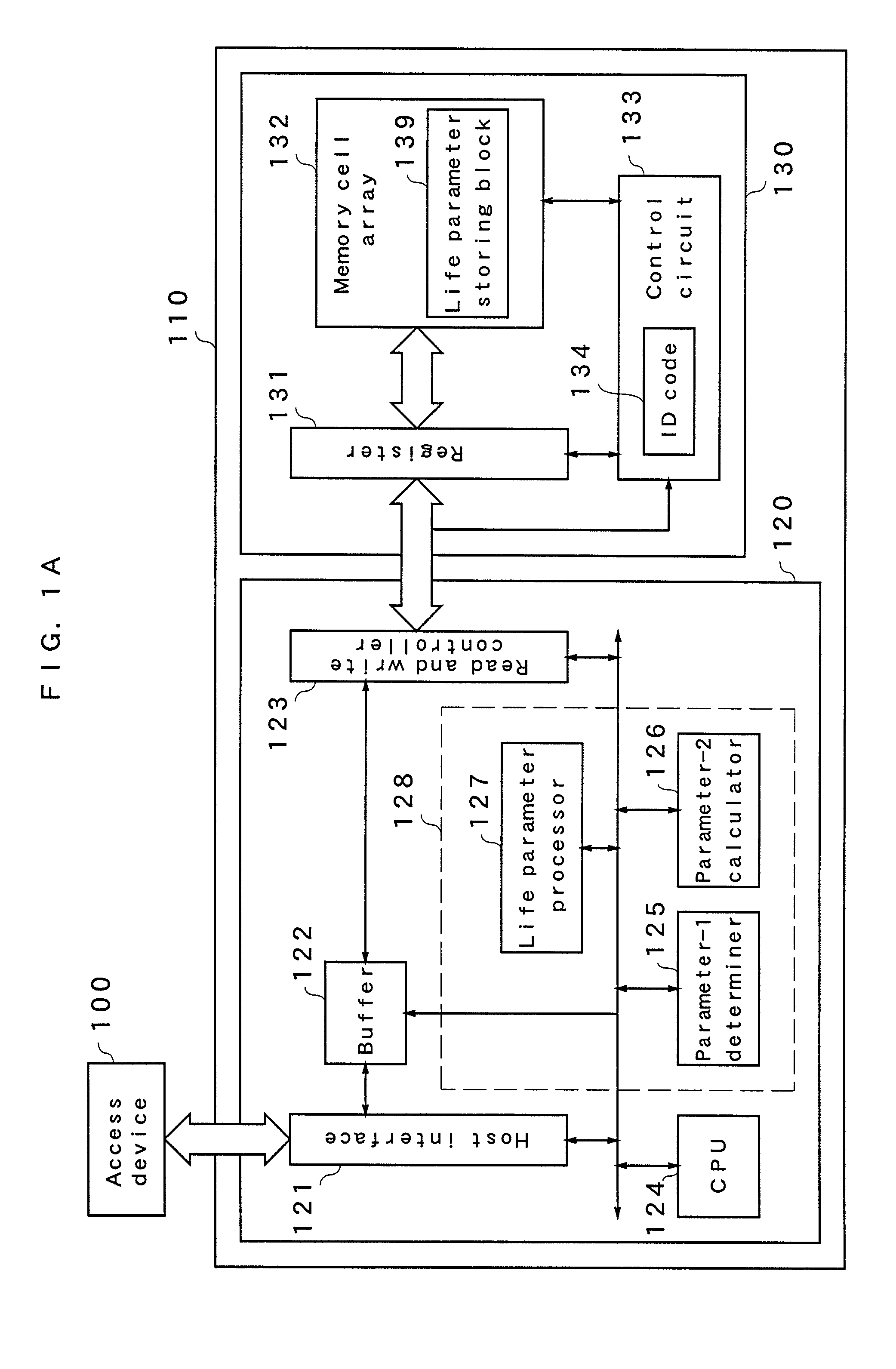
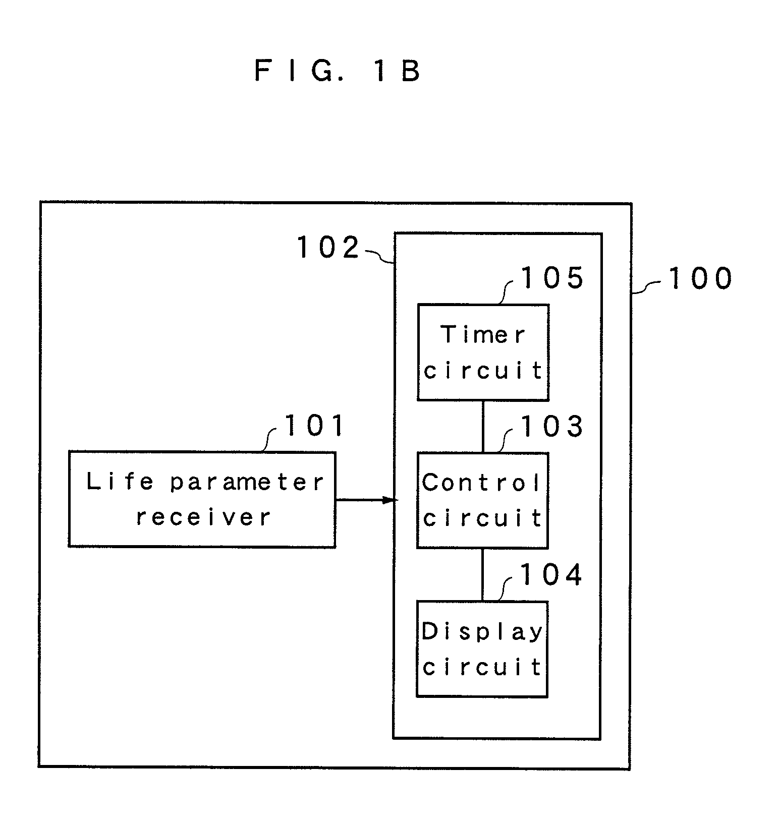
[0071]FIG. 1A is a block diagram showing a nonvolatile memory device in a nonvolatile memory system according to an embodiment of the present invention, and FIG. 1B is a block diagram showing an access device thereof. In FIGS. 1A and 1B, the nonvolatile memory system is so structured as to include an access device 100 and a nonvolatile memory device 110. The access device 100 and the nonvolatile memory device 110 are connected each other by a bus 1. The nonvolatile memory device 110 includes a memory controller 120 and a nonvolatile memory 130. The memory controller 120 and the nonvolatile memory 130 are connected each other via a bus 2.

[0072]The memory controller 120 includes a host interface 121, buffer 122, read and write controller 123, CPU 124, parameter-1 determiner 125, parameter-2 calculator 126, and life parameter processor 127. The parameter-1 determiner 125, parameter-2 calculator 126, and life parameter processor 127 are collectively provided as a life parameter generato...


PUM


Abstract

A life parameter generator generates life parameters related to the life of a nonvolatile memory device by using parameters related to allowable capacity for memory defect and occurrence capacity for memory defect. The life parameters are stored in a life parameter storing block of a nonvolatile memory. An access device reads and displays the stored life parameters. Thus, the user can precisely know the life of the nonvolatile memory device or the moment when a device having a built in nonvolatile memory such as a portable audio becomes unusable.

Description

TECHNICAL FIELD[0001]The present invention relates to a nonvolatile memory device, such as a memory card, provided with a nonvolatile memory, a nonvolatile memory system having an access device added as a component to the nonvolatile memory device, and a defect management method for nonvolatile memory device.BACKGROUND ART[0002]Demands for nonvolatile memory devices provided with a rewritable nonvolatile memory, mainly for semiconductor memory cards, have been growing. Although the semiconductor memory card is very high-priced as compared to an optical disc, a tape media and the like demands for semiconductor memory cards as recording media for a mobile device such as a digital still camera, a mobile phone, or the like have been growing due to its advantages such as small size, light weight, shock resistance, convenience to handle, etc. This semiconductor memory card includes a flash memory as a nonvolatile main memory, and has a memory controller for controlling it. The memory cont...

Claims


Application Information

Patent Timeline
Patent Type & Authority Patents(United States)
IPC IPC(8): G11C29/00
CPCG11C16/349G06F11/008
Inventor NAKANISHI, MASAHIRO
Owner PANASONIC CORP
Learn More