RF power transistor structure and a method of forming the same
- Summary
- Abstract
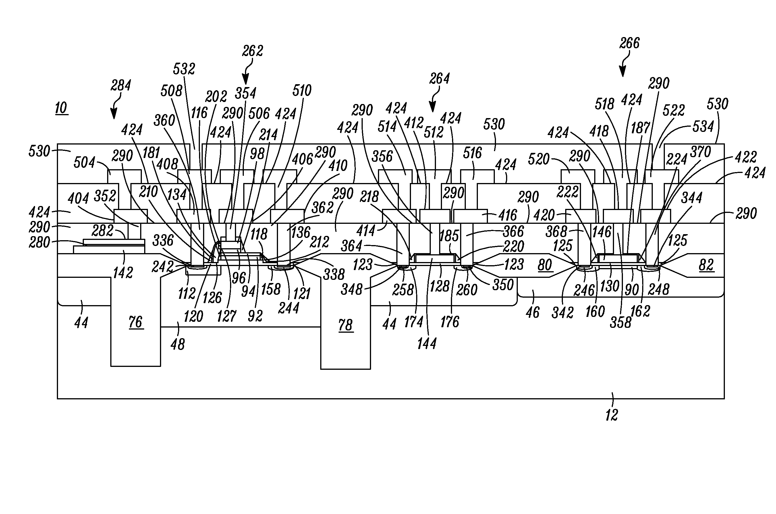
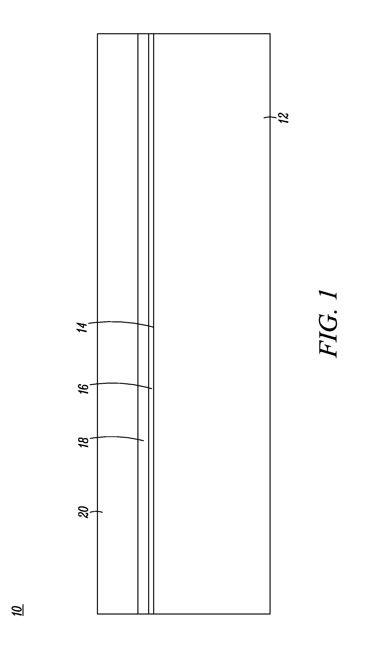
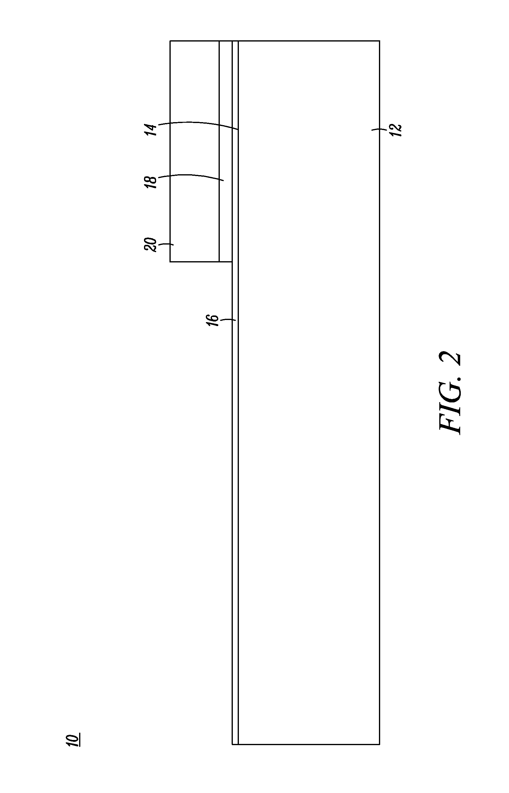
- Description
- Claims
- Application Information
AI Technical Summary
Problems solved by technology
Method used
Image

Examples
Embodiment Construction
In the following description and claims, the terms “comprise” and “include,” along with their derivatives, may be used and are intended as synonyms for each other. In addition, in the following description and claims, the terms “coupled” and “connected,” along with their derivatives, may be used. “Connected” may be used to indicate that two or more elements are in direct physical or electrical contact with each other. “Coupled” may mean that two or more elements are in direct physical or electrical contact. However, “coupled” may also mean that two or more elements are not in direct contact with each other, but yet still co-operate or interact with each other. For example, “coupled” may mean that two or more elements do not contact each other but are indirectly joined together via another element or intermediate elements. Finally, the terms “on,”“overlying,” and “over” may be used in the following description and claims. “On,”“overlying,” and “over” may be used to indicate that two ...
PUM
 Abstract
Description
Claims
Application Information
 - R&D
- Intellectual Property
- Life Sciences
- Materials
- Tech Scout
- Unparalleled Data Quality
- Higher Quality Content
- 60% Fewer Hallucinations
Browse by: Latest US Patents, China's latest patents, Technical Efficacy Thesaurus, Application Domain, Technology Topic, Popular Technical Reports.
© 2025 PatSnap. All rights reserved.Legal|Privacy policy|Modern Slavery Act Transparency Statement|Sitemap|About US| Contact US: help@patsnap.com