
High voltage generation and control in source-side injection programming of non-volatile memory

a non-volatile memory, high-voltage technology, applied in static storage, digital storage, instruments, etc., can solve problems such as difficulties in memory array use, and achieve the effect of low operating voltage and low operating voltage circuitry

Active Publication Date: 2011-02-22
SANDISK TECH LLC
View PDF20 Cites 9 Cited by
  • Summary
  • Abstract
  • Description
  • Claims
  • Application Information

AI Technical Summary

Problems solved by technology

A problem arises when it's desired to program one cell on a word line without programming other cells connected to the same word line.
Although SSI programming offers some improvements over FN programming, its use in an array of memory cells can present difficulties.

Method used


Image

  • High voltage generation and control in source-side injection programming of non-volatile memory
  • High voltage generation and control in source-side injection programming of non-volatile memory
  • High voltage generation and control in source-side injection programming of non-volatile memory

Examples


Embodiment Construction

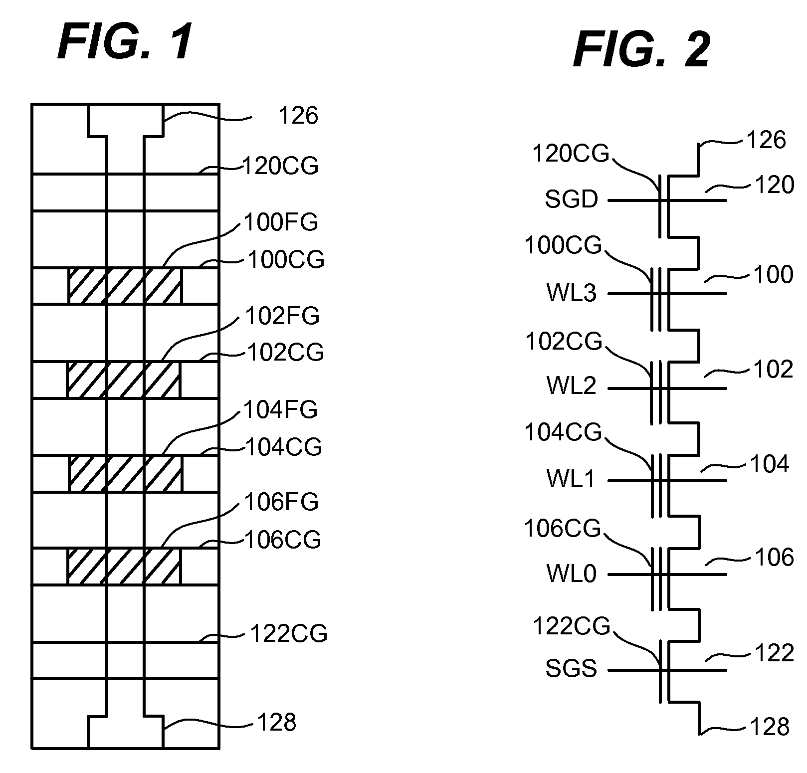
[0039]FIG. 4 is a block diagram of one embodiment of a flash memory system that can be used to implement one or more embodiments of the present disclosure. FIG. 4 is exemplary as other systems can be used in accordance with various implementations. Memory cell array 202 is controlled by column control circuitry 204, row control circuitry 206, c-source control circuitry 208 and p-well control circuitry 208. Column control circuitry 204 is connected to the bit lines of memory cell array 202 for reading data stored in the memory cells, for determining a state of the memory cells during a program operation, and for controlling potential levels of the bit lines to promote or inhibit programming and erasing. Row control circuitry 206 is connected to the word lines to select one of the word lines, to apply read voltages, to apply program voltages combined with the bit line potential levels controlled by column control circuitry 204, and to apply an erase voltage. C-source control circuitry...


PUM


Abstract

Non-volatile memory is programmed using source side hot electron injection. To generate a high voltage bit line for programming, the bit line corresponding to a selected memory cell is charged to a first level using a first low voltage. A second low voltage is applied to unselected bit lines adjacent to the selected bit line after charging. Because of capacitive coupling between the adjacent bit lines and the selected bit line, the selected bit line is boosted above the first voltage level by application of the second low voltage to the unselected bit lines. The column control circuitry for such a memory array does not directly apply the high voltage and thus, can be designed to withstand lower operating voltages, permitting low operating voltage circuitry to be used.

Description

BACKGROUND OF THE INVENTION[0001]1. Field of the Invention[0002]The present disclosure relates to programming in non-volatile memory.[0003]2. Description of the Related Art[0004]Semiconductor memory devices have become more popular for use in various electronic devices. For example, non-volatile semiconductor memory is used in cellular telephones, digital cameras, personal digital assistants, mobile computing devices, non-mobile computing devices and other devices. Electrical Erasable Programmable Read Only Memory (EEPROM), including flash EEPROM, and Electronically Programmable Read Only Memory (EPROM) are among the most popular non-volatile semiconductor memories.[0005]EEPROM and EPROM memories utilize a floating gate that is positioned above and insulated from a channel region in a semiconductor substrate. The floating gate is positioned between source and drain regions. A control gate is provided over and insulated from the floating gate. The threshold voltage of the transistor ...

Claims


Application Information

Patent Timeline
Patent Type & Authority Patents(United States)
IPC IPC(8): G11C16/04
CPCG11C11/5628G11C16/0483G11C16/10G11C16/24G11C16/3418G11C2211/565
Inventor LEE, DANASO, HOCK
Owner SANDISK TECH LLC
Learn More