
Electroluminescent element and light-emitting device

a technology of light-emitting device and electroluminescent element, which is applied in the direction of discharge tube luminescnet screen, natural mineral layered products, transportation and packaging, etc., can solve the problems of difficult control of white balance, poor color conversion efficiency of blue to red, and deterioration of contrast from light emission in pixels, etc., to achieve easy control

Inactive Publication Date: 2011-01-04
SEMICON ENERGY LAB CO LTD
View PDF51 Cites 13 Cited by
  • Summary
  • Abstract
  • Description
  • Claims
  • Application Information

AI Technical Summary

Benefits of technology

[0012]It is an object of the present invention to provide an electroluminescent element which can be easily controlled the color balance in white light emission (white balance).
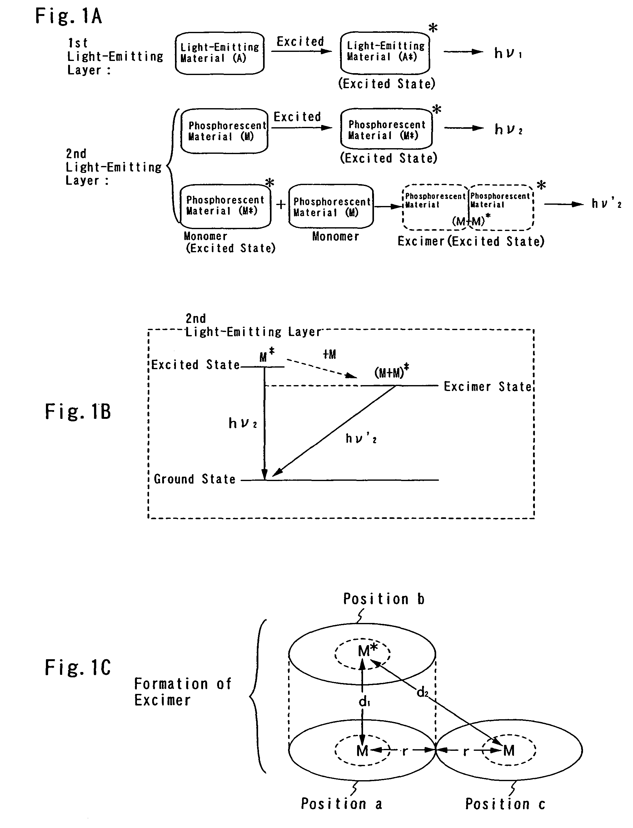
[0013]As the result of research for solving the above mentioned problems, the inventor found that the rate of changes of peak intensity becomes hardly changed depending on light-emitting materials even when a current density is increased by keeping the concentration of light-emitting materials among a plurality of light-emitting materials used for obtaining white light emission in a certain range.
[0016]As stated above, the first light-emitting layer exhibiting blue emission and the second light-emitting layer exhibiting green and red (or orange) emission are formed separately. In consequence, there is an advantage that the electroluminescent element becomes easy to manufacture since the control of the concentration or the like for forming the first light-emitting layer becomes facilitated. Further, compared with the case that all color emission is obtained from one light-emitting layer, it can be expected that the varies of emission wavelength, the decrease of peak intensity, or the like due to the interaction of molecules having different structures from each other (exciplex) within a light-emitting layer is prevented.
[0017]Further, by doping phosphorescent materials into the second light-emitting layer within the above described concentration ranges, not only the number of excimer formed from phosphorescent materials can be controlled, but also the light emission (green emission and red emission) can be obtained from the second light-emitting layer simultaneously with blue emission from the first light-emitting layer. In this case, the peak intensity of phosphorescent emission (green emission) obtained from phosphorescent materials and emission (red (or orange)) from excimer (the peak intensity of both the emission can be considered to be the same because the intensity ratio is depending on the concentration) and the peak intensity of blue emission from the first light-emitting layer changes at the almost same rate in case of increasing current density, hence, the peak intensity is easy to control and white light emission with well white balanced can be easily obtained.
[0028]Accordingly, an electroluminescent element can be provided which can be controlled easily the color balance in white light emission (white balance) by keeping the concentration so as to be within a certain range of light-emitting materials among a plurality of light-emitting materials used for obtaining white light emission.

Problems solved by technology

However, in case of adopting the CCM method, there has been a problem in red color since color conversion efficiency of from blue to red is poor in principle.
In addition, there has been a problem that the contrast becomes deteriorated from light emission in pixels due to outside light such as sunlight since color conversion materials are fluorescent materials.
Consequently, it becomes extremely difficult to control white balance which is adjusted by the parameter which determines the peak intensity of these emission colors.

Method used


Image

  • Electroluminescent element and light-emitting device
  • Electroluminescent element and light-emitting device
  • Electroluminescent element and light-emitting device

Examples


embodiment 1

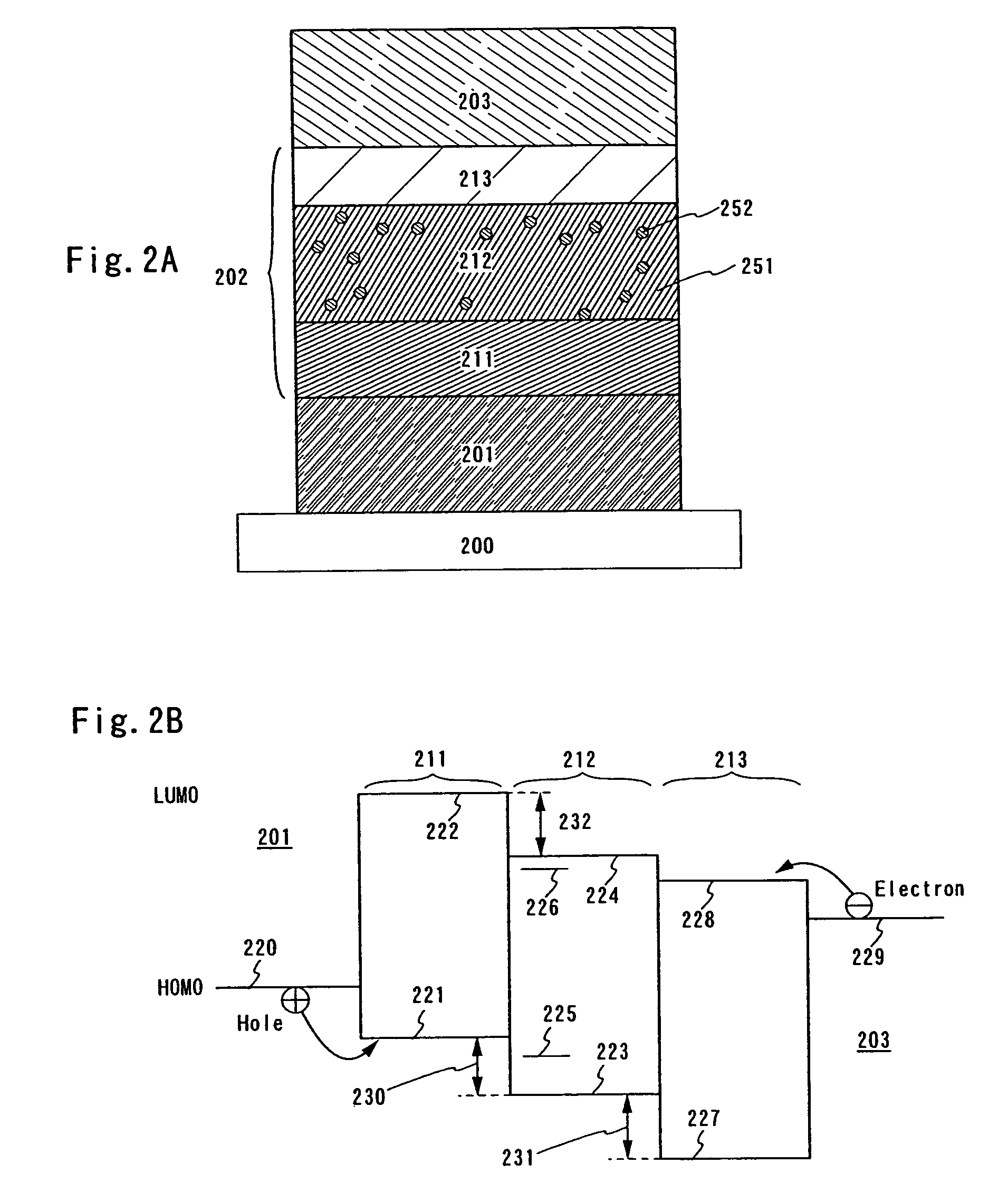
[0049]In Embodiment 1, as shown in FIG. 2A, the case that a first electrode 201, an electroluminescent layer 202, and a second electrode 203 are formed over a substrate 200, and that the electroluminescent layer 202 has a lamination structure comprising a first light-emitting layer 211, a second light-emitting layer 212, and an electron transporting layer 213 will be explained. In addition, the first light-emitting layer 211 includes a light-emitting body. The second light-emitting layer 212 comprises host materials 251 and phosphorescent materials 252 which serve as a light-emitting body. The phosphorescent materials can generate both phosphorescent emission and excimer emission.

[0050]As a light-emitting body (light-emitting material) for the first light-emitting layer 211, blue fluorescent materials having hole transportation properties such as N,N′-bis(3-methylphenyl)-N,N′-diphenyl-1,1′-biphenyl-4,4′-diamine (abbreviated TPD) or derivatives thereof such as 4,4′-bis[N-(1-naphthyl)...

embodiment 2

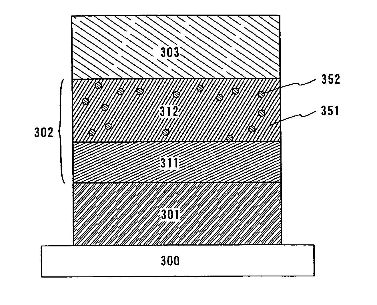
[0064]In Embodiment 2, the case that a first electrode 301, an electroluminescent layer 302, and a second electrode 303 are formed over a substrate 300, and the electroluminescent layer 302 has a lamination structure comprising a first light-emitting layer 311 and a second light-emitting layer 312 will be explained with reference to FIG. 3A. In addition, second light-emitting layer 312 comprises host materials 351 and phosphorescent materials 352. The phosphorescent materials can generate phosphorescent emission and excimer emission.

[0065]Embodiment 2 is distinguished from Embodiment 1 by the fact that the electroluminescent layer does not comprise the electron transporting layer, and so Embodiment 2 has an advantage that the process for forming the electron transporting layer can be omitted. In addition, materials having excellent electron transportation properties are preferably used as host materials 321 for the second light-emitting layer 312 in order to keep luminous efficiency...

embodiment 3

[0070]In Embodiment 3, the case that a first electrode 401, an electroluminescent layer 402, and a second electrode 403 are formed over a substrate 400, and that the electroluminescent layer 402 has a lamination structure comprising a hole injecting layer 411, a first light-emitting layer 412, and a second light-emitting layer 413, and an electron transporting layer 414 will be explained with reference to FIG. 4A. In addition, second light-emitting layer 413 comprises host materials 451 and phosphorescent materials 452 that serve as a light-emitting body. The phosphorescent materials can generate phosphorescent emission and excimer emission.

[0071]As materials for the hole injecting layer 411, besides the above described hole transporting materials such as TPD, α-NPD, TDATA, or MTDATA, the following hole transporting materials can be used.

[0072]As hole injection materials, porphyrin compounds are useful among other organic compounds such as phthalocyanine (abbreviated H2-Pc), copper ...


PUM

PropertyMeasurementUnit
Fractionaaaaaaaaaa
Thicknessaaaaaaaaaa
Thicknessaaaaaaaaaa

Abstract

An electroluminescent element which can easily control the balance of color in white emission (white balance) is provided according to the present invention. The electroluminescent element comprises a first light-emitting layer containing one kind or two or more kinds of light-emitting materials, and a second light-emitting layer containing two kinds of light-emitting materials (a host material and a phosphorescent material) in which the phosphorescent material is doped at a concentration of from 10 to 40 wt %, preferably, from 12.5 to 20 wt %. Consequently, blue emission can be obtained from the first light-emitting layer and green and red (or orange) emission can be obtained from the second light-emitting layer. An electroluminescent element having such device configuration can easily control white balance since emission peak intensity changes at the same rate in case of increasing a current density.

Description

BACKGROUND OF THE INVENTION[0001]1. Field of the Invention[0002]The present invention relates to an electroluminescent element comprising an anode, a cathode, and a layer including organic compounds (hereinafter, an electroluminescent layer) which emit light by applying current through the pair of electrodes; and a light-emitting device which comprises the electroluminescent layer. More specifically, this invention relates to an electroluminescent element which exhibits white light emission, and a full color light-emitting device comprising the electroluminescent element.[0003]2. Related Art[0004]An electroluminescent element comprises an electroluminescent layer interposed between a pair of electrodes (anode and cathode). The emission mechanism is as follows. Upon applying voltage through the pair of electrodes, holes injected from an anode and electrons injected from a cathode are recombined with each other within the electroluminescent layer to result in the formation of molecula...

Claims


Application Information

Patent Timeline
IPC IPC(8): B32B7/02H01J1/62C09K11/06H01L51/00H01L51/30H01L51/50H05B33/12H05B33/14H05B33/20
CPCC09K11/06H01L51/0087H01L51/5016H01L51/5036H05B33/14H01L51/504Y10T428/24942C09K2211/185H01L51/0052H01L51/0059H01L51/0077H01L51/0081H01L51/0085Y02B20/181Y10S428/917C09K2211/1074C09K11/025Y02B20/00H10K85/615H10K85/631H10K85/30H10K85/324H10K85/346H10K85/342H10K50/11H10K2101/10H10K50/125H10K59/8051H10K59/873H10K59/8052H10K77/111H10K50/13H10K50/81H10K50/82H10K50/844H10K85/626H10K85/633H10K85/6572C09K2211/1007C09K2211/1029
Inventor ABE, HIROKO
Owner SEMICON ENERGY LAB CO LTD
Learn More