Color image display panel and driving method thereof
a technology of color image and display panel, which is applied in the direction of optics, instruments, static indicating devices, etc., can solve the problems of increasing process costs, reducing the opening ratio of pixels, and providing excessive information unnecessary for human vision, so as to facilitate the production of the second optical modulating layer, improve the opening ratio, and achieve sufficient bright/dark display resolving power.
- Summary
- Abstract
- Description
- Claims
- Application Information
AI Technical Summary
Benefits of technology
Problems solved by technology
Method used
Image
Examples
example 1
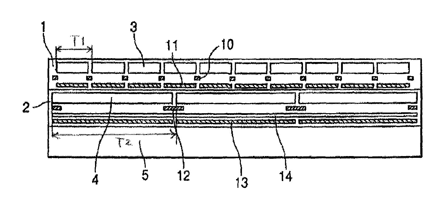
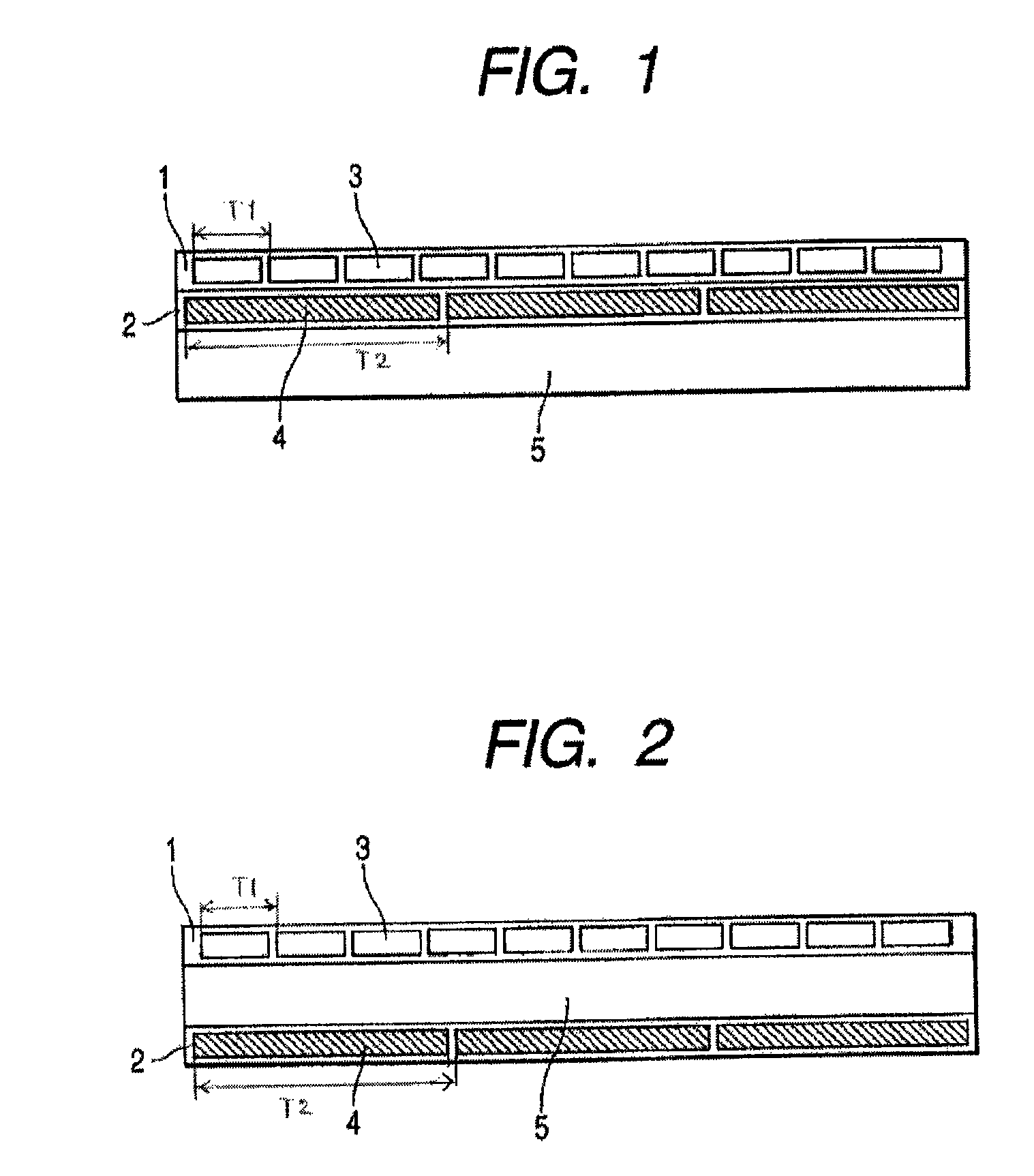
[0054]In the following, a specific example of the color image display panel of the present invention, having a configuration shown in FIG. 1, will be explained with reference to FIG. 6. It is to be noted that the present invention is not limited to such example.
[0055]A polyester film of a thickness of 200 μm was washed, and an aluminum layer was deposited thereon and was subjected to a photolithographic process to prepare drive electrodes 13 of a width of 330 μm, with a spacing of 10 μm. Their surface was covered with a two-liquid curable acrylic resin layer of 1 μm, and then an urethane resin layer, in which a titanium oxide white pigment was dispersed, was formed with a thickness of 8 μm to constitute a scattering reflection layer 14. Again the two-liquid curable acrylic resin layer was applied by 1 μm, and then an aluminum layer was deposited and subjected to a photolithographic process to form a stripe-shaped common electrode 12 of a width of 10 μm. Utilizing a photolithography ...
example 2
[0059]FIG. 8 is a functional block diagram of a paper display utilizing an electrophoretic display apparatus of the invention, and an equipment system utilizing such paper display.
[0060]The functional blocks are mainly divided into two, one being a paper display module 81 and the other being a paper display system module 82.
[0061]The paper display module 81 is constituted of a paper display element array 83, a driving backplane 84, a drive circuit (X) 85 and a drive circuit (Y) 86, and a panel controller (not shown) may be additionally provided for supplying the driving backplane 84 and the drive circuits 85, 86 with an electric power and signals. An interface module 87 may also serve as such panel controller. Also a temperature detecting element (not shown) such as a thermocouple or a thermistor may be provided for a temperature compensation control. Also the paper display module 81 may include a digitizer 88. Such digitizer can be of various types, such as an electromagnetic induc...
PUM
| Property | Measurement | Unit |
|---|---|---|
| width | aaaaa | aaaaa |
| width | aaaaa | aaaaa |
| thickness | aaaaa | aaaaa |
Abstract
Description
Claims
Application Information
 - R&D
- Intellectual Property
- Life Sciences
- Materials
- Tech Scout
- Unparalleled Data Quality
- Higher Quality Content
- 60% Fewer Hallucinations
Browse by: Latest US Patents, China's latest patents, Technical Efficacy Thesaurus, Application Domain, Technology Topic, Popular Technical Reports.
© 2025 PatSnap. All rights reserved.Legal|Privacy policy|Modern Slavery Act Transparency Statement|Sitemap|About US| Contact US: help@patsnap.com


