
Sample hold circuit for use in time-interleaved A/D converter apparatus including paralleled low-speed pipeline A/D converters

a technology of time-interleaved a/d converter and sample hold circuit, which is applied in the direction of pulse manipulation, pulse technique, instruments, etc., can solve the problems of series connection addition, significant deterioration of the performance of the time-interleaved a/d converter, etc., to achieve the effect of reducing the clock skew, increasing the chip area and small area

Inactive Publication Date: 2010-11-16
SEMICON TECH ACADEMIC RES CENT
View PDF13 Cites 26 Cited by
  • Summary
  • Abstract
  • Description
  • Claims
  • Application Information

AI Technical Summary

Benefits of technology

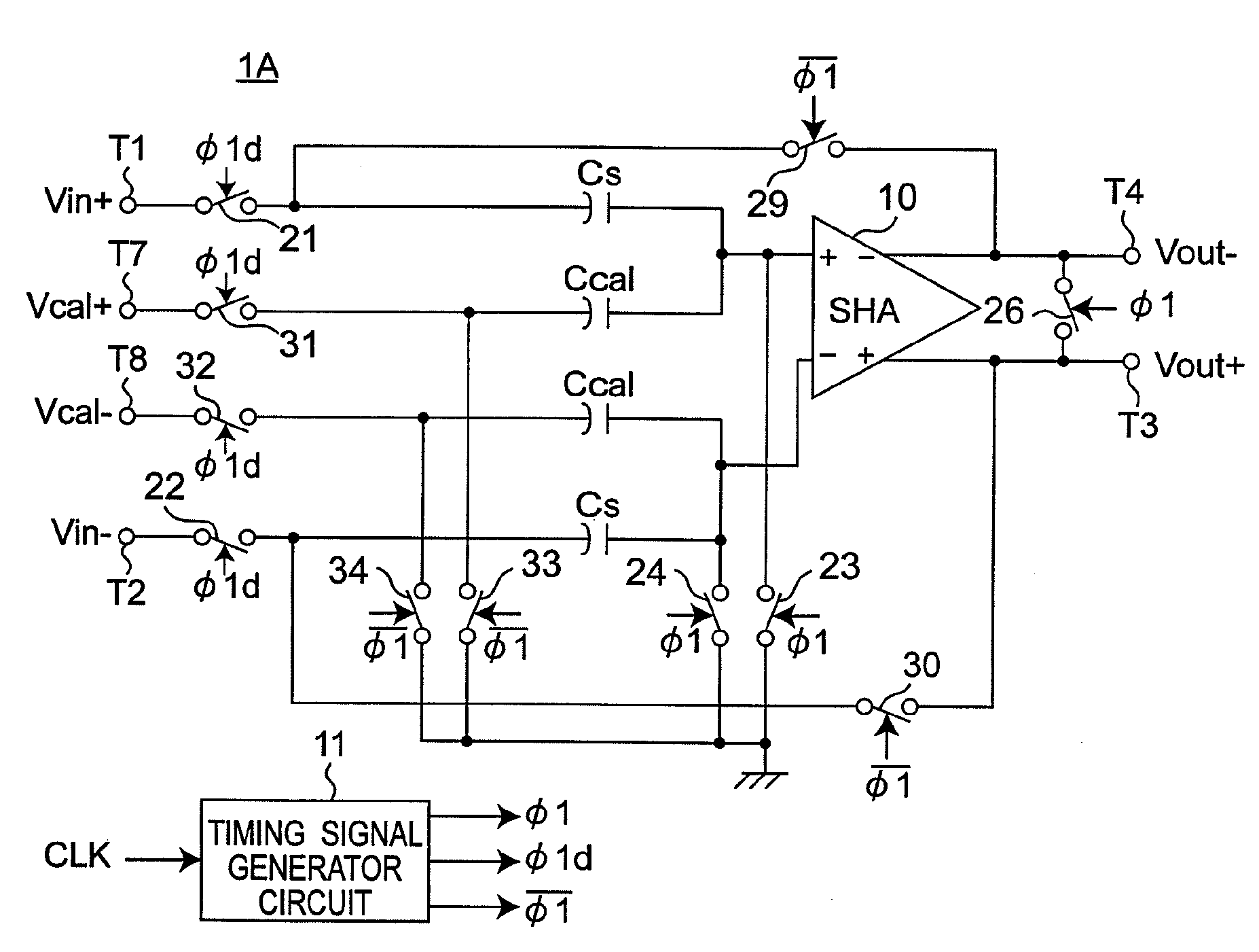
[0034]According to the sample hold circuit of the present invention, the sample hold circuit includes the adder circuit that adds the ramp calibration signal to the input signal by inputting the ramp calibration signal generated to have a frequency identical to that of the sampling clock signal and a predetermined slope based on the sampling clock signal to the sample hold amplifier via the calibration capacitor having a capacitance smaller than the capacitance of the sampling capacitor. The calculator device calculates the differential signal between the respective output signals from the respective A / D converters. With this arrangement, the ramp calibration signal is sampled as a DC value corresponding to the amount of clock skew between the sample hold circuits when it is sampled by the sample hold circuit, and the differential signal represents the amount of clock skew, and this leads to measurement of the amount of clock skew. Accordingly, this leads to the provision of the sample hold circuit capable of measuring the amount of clock skew more extremely simply and more stably than those of the prior art technique without any reference voltage source but inputting the calibration signal. In addition, the present invention can provided the A / D converter apparatus that employs the same sample hold circuit.
[0035]Moreover, the phase of the clock signal can be adjusted so as to minimize the clock skew based on the measured clock skew. In particular, the A / D converter apparatus having the circuit for measuring the amount of clock skew includes the small calibration capacitor and the switch device that branches from the sample hold circuit. The additional calibration capacitor, which slightly increases the chip area, does not exert a large influence on the other circuit area. Therefore, a clock skew measurement circuit can be configured with an extremely small area.

Problems solved by technology

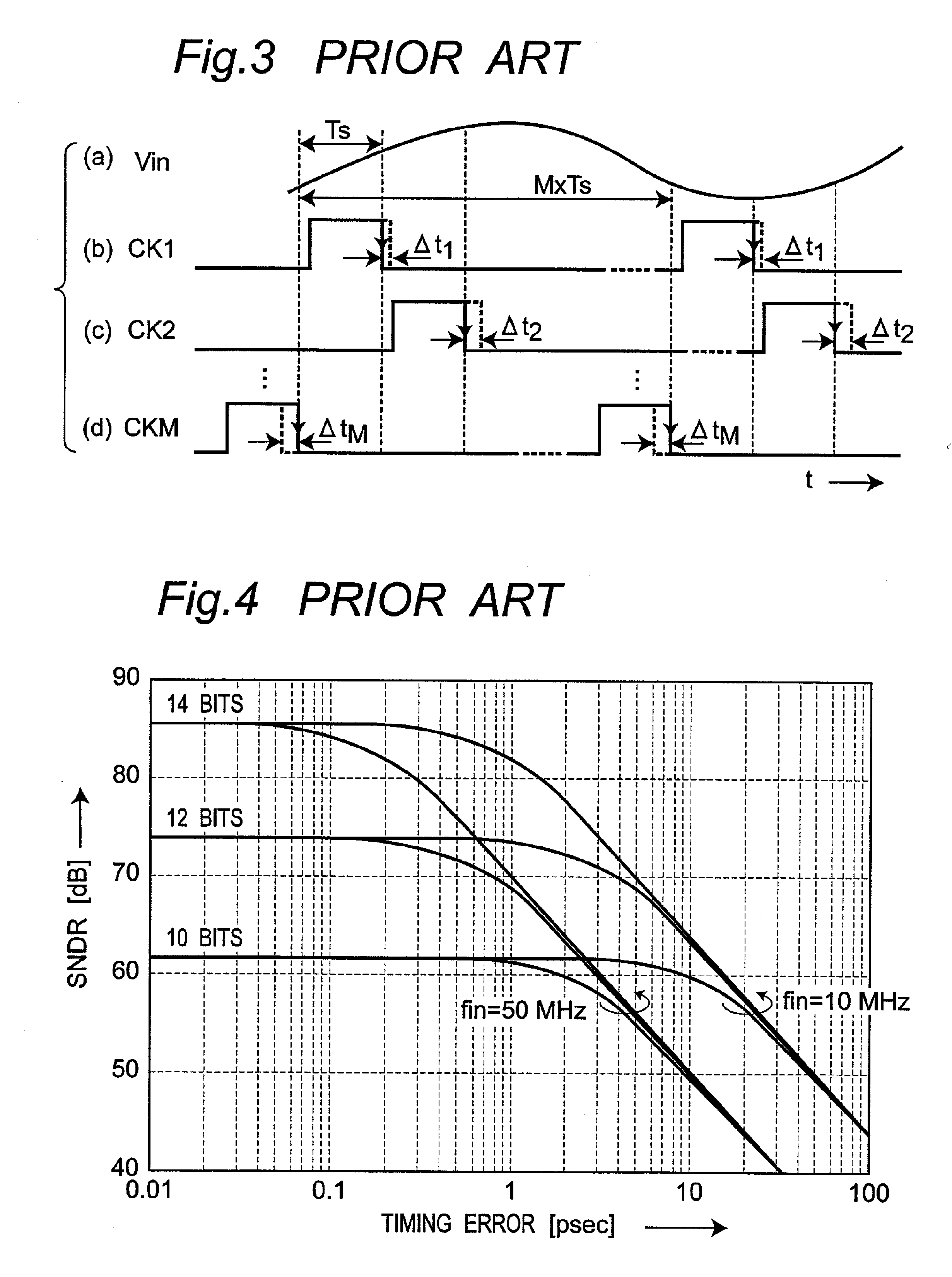
However, since the sampling is performed practically in positions different from the ideal ones as indicated in FIG. 3 due to mismatch between channels, the clock skew occurs and becomes a factor to significantly deteriorate the performance of the time-interleaved A / D converter.
However, the sample hold amplifier must operate at the maximum rate thereof, and this leads to the problem of difficulties in its being applied to a high-speed and high-resolution A / D converter.
However, the method has the defects that a sampling switch of a series connection is added and a tracking time is short.
A calibration method on the background is now under researches due to the fact that the sampling of the clock skew is difficult during device operation.
Regarding the calibration of RC mismatch, sufficient researches have not been performed yet.
The method is impractical because the load connected to the voltage source of the reference voltage is generally large and has had the problem of reference voltage fluctuations during the time-interleaved A / D conversion.
Moreover, the prior art blind estimation method, which needs no calibration signal, has its algorithm generally complicated and a problem that a large amount of data is necessary for convergence.

Method used


Image

  • Sample hold circuit for use in time-interleaved A/D converter apparatus including paralleled low-speed pipeline A/D converters
  • Sample hold circuit for use in time-interleaved A/D converter apparatus including paralleled low-speed pipeline A/D converters
  • Sample hold circuit for use in time-interleaved A/D converter apparatus including paralleled low-speed pipeline A/D converters

Examples


Embodiment Construction

[0053]Preferred embodiments of the present invention will be described with reference to the drawings. In the following preferred embodiments, like components are denoted by like reference numerals.

[0054]FIG. 6 is a timing chart showing an operation in presence and absence of skew in an A / D converter according to one preferred embodiment of the present invention. FIG. 7 is a block diagram showing a configuration of a sample hold circuit 1A for use in the A / D converter of the present preferred embodiment, and

[0055]FIG. 8 is a timing chart showing timing signals φ, φ1d, and φ1 generated by the timing signal generator circuit 11 of FIG. 7.

[0056]In the preferred embodiment of the present invention, a novel practical adder circuit (see FIGS. 7, 10, and 11) of a calibration signal for use in the sample hold circuit of the A / D converter apparatus. Referring to FIG. 6, a clock skew amount (in FIG. 6, Vcal,m (m=1, 2, . . . , M) is a detected voltage corresponding to the clock skew amount) is...


PUM


Abstract

A sample hold circuit is provided for use in a time-interleaved A / D converter apparatus including a plurality of low-speed pipeline A / D converters which are parallelized. The sample hold circuit includes a sampling capacitor and a sample hold amplifier, and operates to sample and hold an input signal by using a switched capacitor. An adder circuit of the sample hold circuit adds a ramp calibration signal to the input signal, by inputting the ramp calibration signal generated to have a frequency identical to that of a sampling clock signal and a predetermined slope based on the sampling clock signal, into a sample hold amplifier via a calibration capacitor having a capacitance smaller than that of the sampling capacitor.

Description

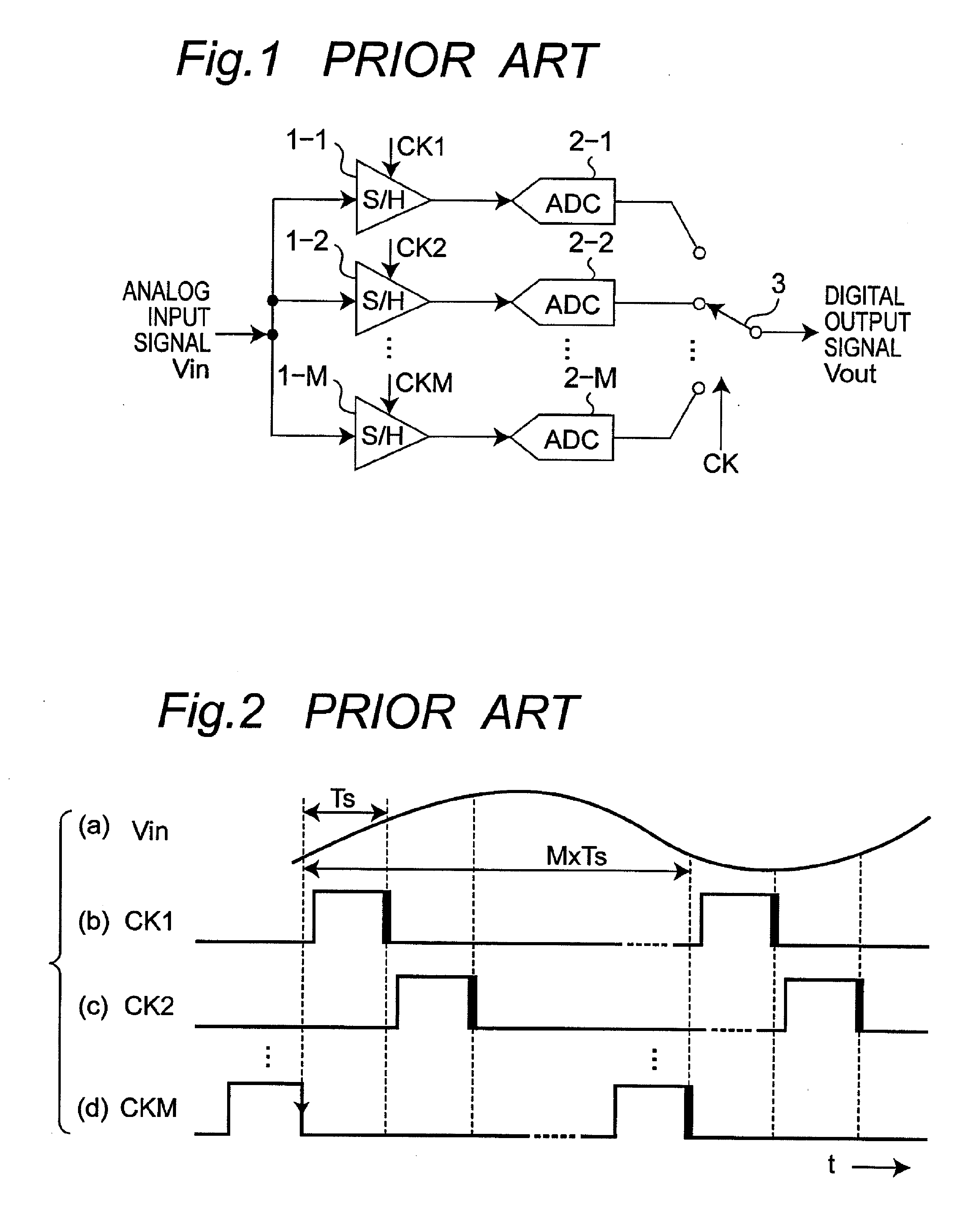
BACKGROUND OF THE INVENTION[0001]1. Field of the Invention[0002]The present invention relates to a sample hold circuit for use in a time-interleaved A / D converter, and in particular, to a sample hold circuit for use in a time-interleaved A / D converter including a plurality of low-speed pipeline A / D converters which are parallelized, and a time-interleaved A / D converter apparatus utilizing the same sample hold circuit.[0003]2. Description of the Related Art[0004]A time-interleaved A / D converter including a plurality of low-speed pipeline A / D converters which are parallelized is an architecture capable of achieving high-speed sampling.[0005]FIG. 1 is a block diagram showing a configuration of a prior art time-interleaved A / D converter, and FIG. 2 is a timing chart showing an operation of the A / D converter of FIG. 1. FIG. 3 is a timing chart showing an operation of the A / D converter of FIG. 1 when a clock skew occurs.[0006]Referring to FIG. 1, an analog input signal Vin is inputted to ...

Claims


Application Information

Patent Timeline
Patent Type & Authority Patents(United States)
IPC IPC(8): H03M1/10
CPCG11C27/026H03M1/1009H03M1/1215
Inventor KAWAHITO, SHOJILIU, ZHENGSHIMIZU, YASUHIDETANI, KUNIYUKIKURAUCHI, AKIRASUSHIHARA, KOJIMASHIKO, KOICHIRO
Owner SEMICON TECH ACADEMIC RES CENT
Learn More