Power switching circuit improved to reduce loss due to reverse recovery current

a reverse recovery current and power switching technology, applied in the field of power switching circuits, can solve the problems of increasing switching loss and noise, steep time characteristic, and high reverse recovery current flowing through the intrinsic diode, so as to reduce the negative effect of reverse recovery characteristic of the second diode and reduce the amount of minor carries. , the effect of reducing the amount of reverse recovery curren

Active Publication Date: 2010-08-17
DENSO CORP
View PDF4 Cites 16 Cited by
  • Summary
  • Abstract
  • Description
  • Claims
  • Application Information

AI Technical Summary

Benefits of technology

[0016]In view of the circumstances set forth above, an object of an aspect of the present invention is to provide power switching circuits having a simple structure and reducing loss and / or noise due to a diode, such as an intrinsic diode, connected in antiparallel to a switching element.
[0019]Thus, as compared with the structure in which no second inductance is provided in the second commutation path or the second inductance is lower than the first inductance, it is possible to reduce a reverse recovery current through the first diode. This allows the sum of a current flowing through each of the first and second diodes after the commutation period to be immediately reduced. Note that, because the second diode has a reverse recovery characteristic superior than that of the first diode based on the difference between their reverse recovery times, an adverse effect of the reverse recovery characteristic of the second diode is relatively reduced.
[0020]In addition, with the configuration of the one aspect of the present invention, a reverse recovery current that conventionally flowed only the first diode is separated to flow both the first diode and the second diode. This makes it possible to reduce the amount of minor carries charged in the first diode by a forward current flowing through the first diode.
[0021]Accordingly, the power switching circuit of the one aspect of the present invention has a simple structure in which the second inductance and the second diode are connected across the first diode; this simple structure achieves the effects set forth above. This therefore increases the availability of the power switching circuit.

Problems solved by technology

For this reason, when a PN junction diode is used to be connected in antiparallel to such a semiconductor switching element, during the reverse recovery time, the reverse recovery current flows through the diode, resulting in increasing switching loss and noise.
This results in increasing switching loss and noise.
However, when a MOSFET with the super junction structure (SJ) is used as a semiconductor switching element to be installed in a power converter, the reverse recovery current flowing through the intrinsic diode becomes high and has a steep time characteristic.
This results in increasing loss and noise.
However, the approach disclosed in the nonpatent document 1 may complicate the circuit structure consisting of the MOSFET and the diode.
The approach disclosed in the nonpatent document 1 also may create loss due to the forward voltage drop across the anti-series diode upon the MOSFET being on.
Thus, the approach disclosed in each of the US Patent and EP Patent Application Publication may complicate the circuit structure consisting of the MOSFET and the external circuit, and remains loss due to the reverse recovery current based on the low voltage.

Method used


Image

  • Power switching circuit improved to reduce loss due to reverse recovery current
  • Power switching circuit improved to reduce loss due to reverse recovery current
  • Power switching circuit improved to reduce loss due to reverse recovery current

Examples


Embodiment Construction

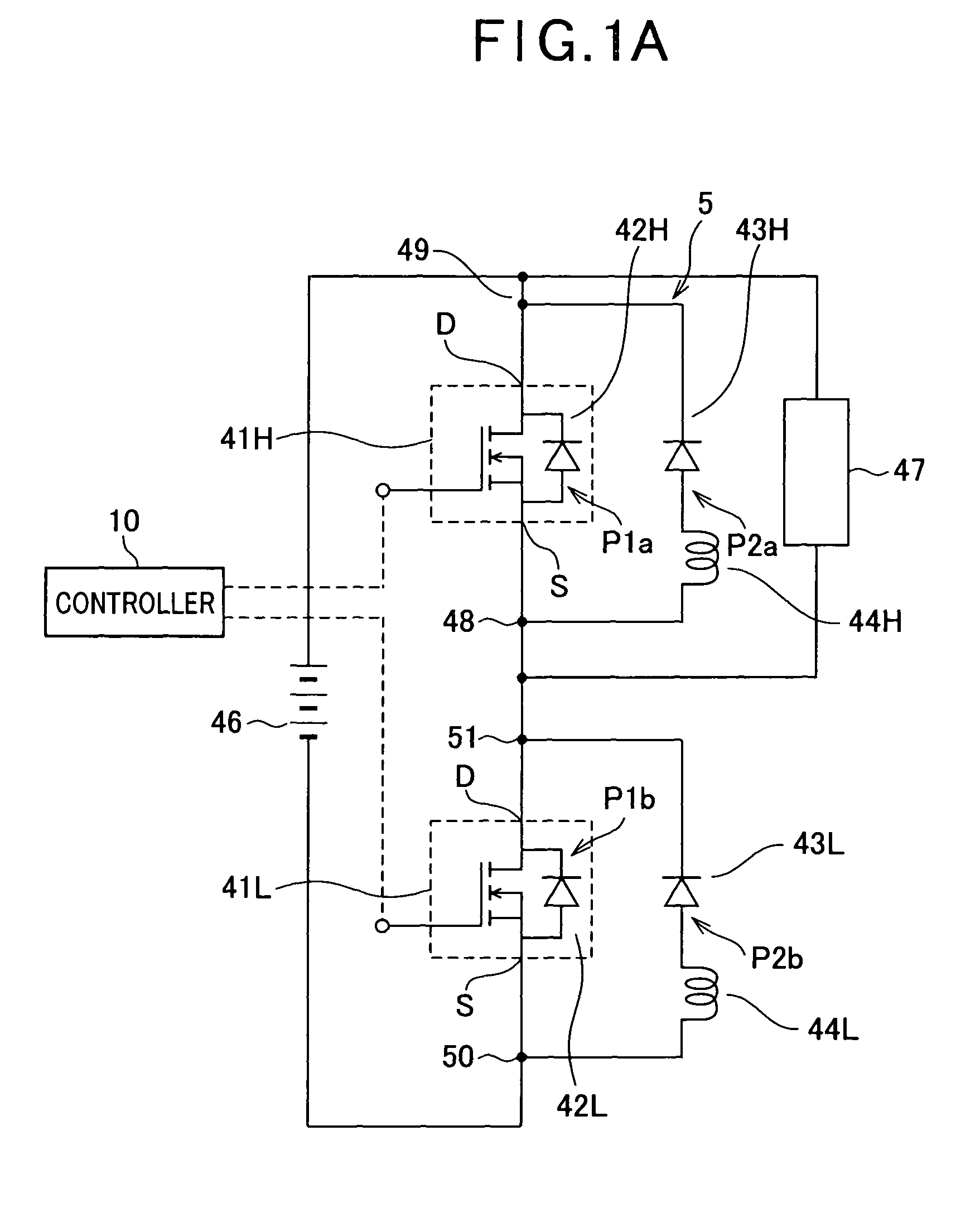
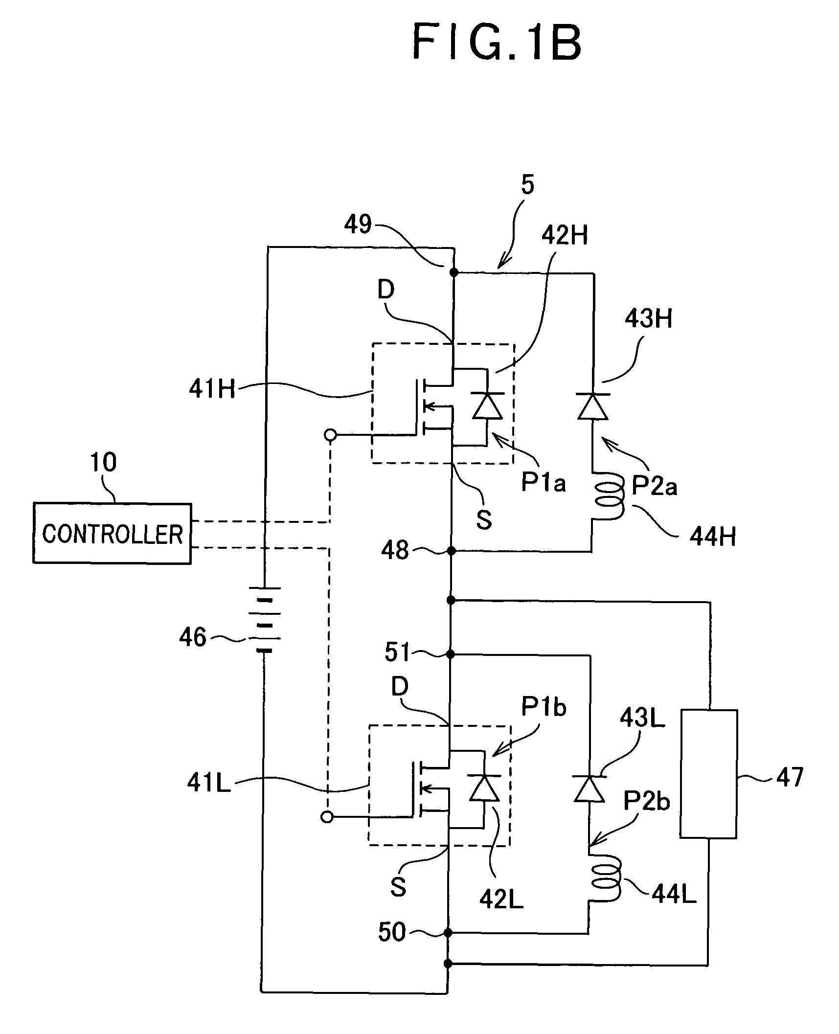
[0041]An embodiment of the present invention will be described hereinafter with reference to the accompanying drawings.

[0042]Referring to FIG. 1A, there is provided a power switching circuit 1 for driving an inductive load 47 according to the embodiment of the present invention.

[0043]The power switching circuit 1 includes a direct current (DC) battery 46 and a half-bridge module 5.

[0044]The half-bridge module 5 includes a pair (bridge arm) of series-connected high-side and low-side MOSFETs 41H and 41L serving as switching elements, intrinsic diodes 42H and 42L of the respective MOSFETs 41H and 41l, and Schottky barrier diodes (Schottky diodes) 43H and 43L. Each of the intrinsic diodes 42H and 42L serves as a first diode (first commutation diode), and each of the Schottky diodes 43H and 43L serves as a second diode (second commutation diode).

[0045]In FIG. 1A, reference character 44H represents an inductance of wiring, and reference character 44L represents an inductance of wiring.

[00...


PUM


Abstract

In a power switching circuit, a second commutation member has a second commutation path electrically connected in parallel to a first commutation path and a second diode provided in the second commutation path and electrically connected antiparallel to a semiconductor switching element. While the semiconductor switching element is off, the second commutation path allows a second current based on the inductive load to flow therethrough in a forward direction of the second diode within a commutation period. The second diode has a second reverse recovery time shorter than a first reverse recovery time of the first diode. A second inductance of the second commutation path is higher than a first inductance of the first commutation path.

Description

CROSS REFERENCE TO RELATED APPLICATIONS[0001]This application is based on Japanese Patent Application 2008-34524 filed on Feb. 15, 2008. The descriptions of the Patent Application are all incorporated herein by reference.FIELD OF THE INVENTION[0002]The present invention relates to power switching circuits with a switching element for switching on and off the switching element to thereby drive inductive loads. More particularly, the present invention relates to such power switching circuits with a diode connected in antiparallel to the switching element; is diode allows a flywheel current to flow therethrough.BACKGROUND OF THE INVENTION[0003]Semiconductor switching elements are installed in a power converter, such as an inverter, for driving inductive loads, such as motors. In order to bypass a current flowing in a semiconductor switching element when the semiconductor switching element is turned off, a diode is connected in antiparallel to the semiconductor switching element. Specif...

Claims


Application Information

Patent Timeline
Patent Type & Authority Patents(United States)
IPC IPC(8): H02H7/122
CPCH02M3/1588H03K17/08142Y02B70/1466H03K17/12H01L2224/0603H01L2224/48137H01L2224/48247H01L2224/49111H01L2924/19107H01L2924/13055H01L2924/13091H01L2924/12032H03K17/14Y02B70/10H01L2924/00
Inventor SASAYA, TAKANARIINOUE, TAKESHIKIMURA, TOMONORI
Owner DENSO CORP
Why Eureka
Try Eureka