CDM performance of high speed CLK inputs

a high-speed clk input and cdm technology, applied in emergency protective arrangements, emergency protective arrangements, electrical equipment, etc., can solve the problems of limiting the input bandwidth, the survivability of this oxide to esd events in 65 nm technologies and beyond, and the increase of the capacitive loading on the pad, so as to reduce the capacitance

Inactive Publication Date: 2010-07-20
ALTERA CORP
View PDF7 Cites 8 Cited by
  • Summary
  • Abstract
  • Description
  • Claims
  • Application Information

AI Technical Summary

Problems solved by technology

While such circuit can be employed in older technologies, where input buffers use relatively thick gate oxides, guaranteeing the survivability of this oxide to ESD events in 65 nm technologies and beyond constitutes a significant challenge.
Of particular concern are charge device model (CDM) discharges where dangerous high voltages can appear directly on the gate of the input buffer.
Any attempt to increase the size of the series diode and or the mosfet clamp with the intent to decrease such voltage overshoots will inevitably lead to an increase of the capacitive loading on the pad limiting the input bandwidth.

Method used


Image

  • CDM performance of high speed CLK inputs
  • CDM performance of high speed CLK inputs
  • CDM performance of high speed CLK inputs

Examples


Embodiment Construction

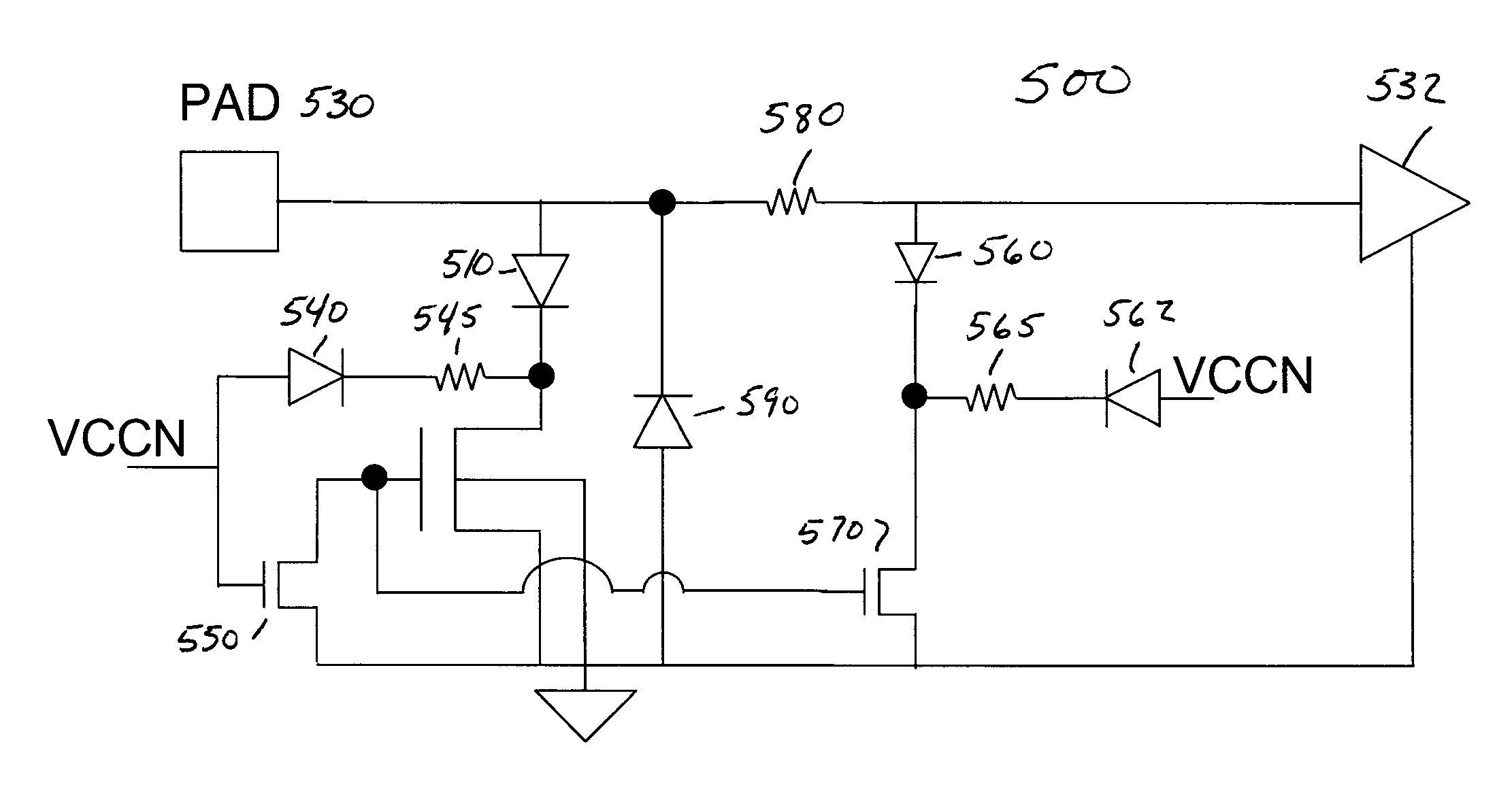
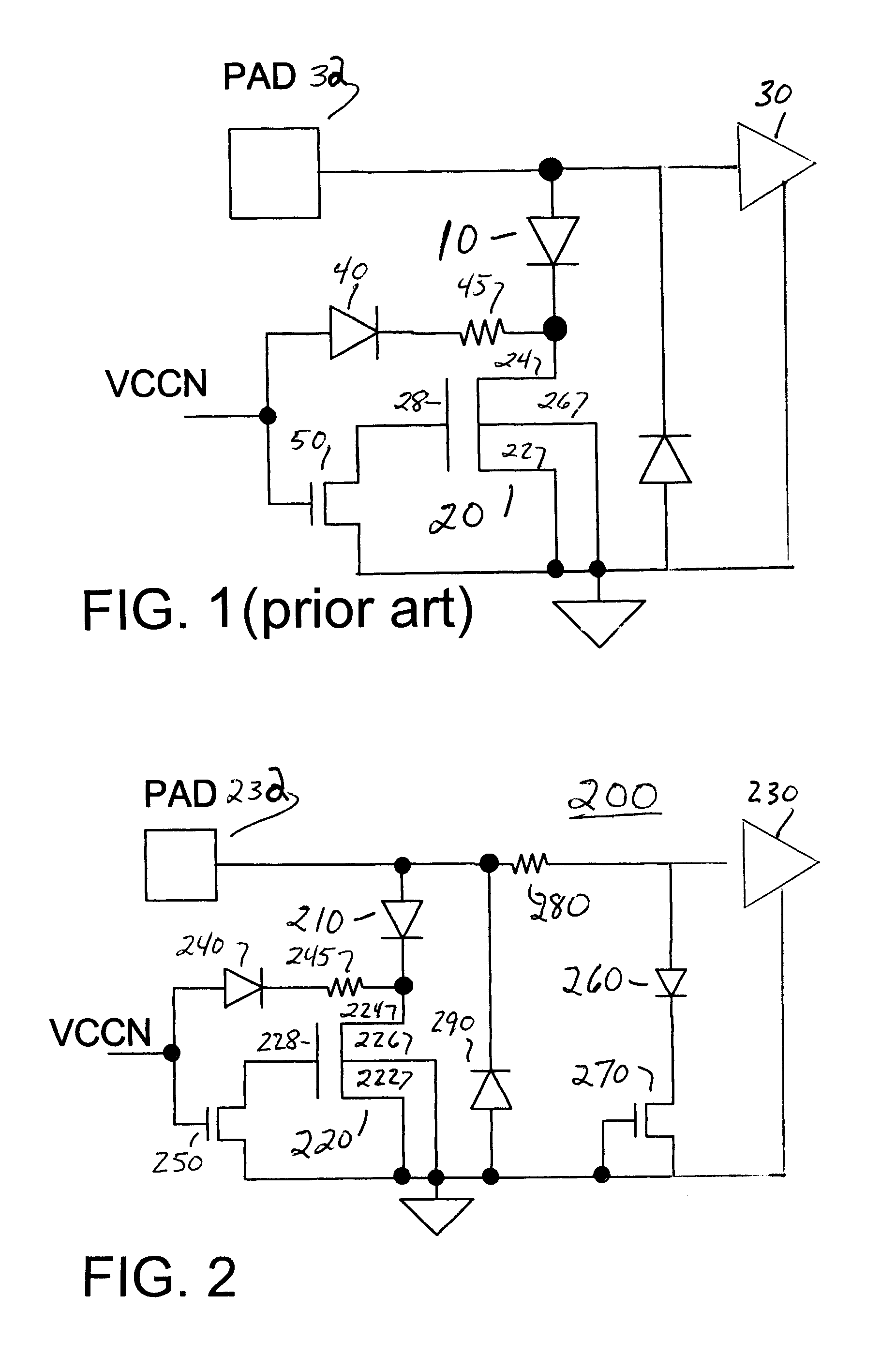
[0012]FIG. 2 is a schematic diagram of an illustrative embodiment of an ESD circuit 200 of the present invention. Circuit 200 comprises an input buffer 230 connected to a pad or node 232, a diode 210 and main clamp 220 connected between pad or node 232 and ground, and a diode 260, secondary clamp 270 and isolation resistance 280 connected in series between the pad and ground. Main clamp 220 is an MOS transistor comprising a source 222, a drain 224, a body 226 and a gate 228. Source 222 and body 226 are connected to ground; and drain 224 is connected to the cathode of diode 210. The anode of diode 210 is connected to pad 232. Preferably, the drain of the main clamp is pulled to Vcc by diode 240 and resistor 245 to avoid forward biasing diode 210; and gate 228 of the main clamp is soft grounded through a transistor 250 to facilitate bipolar triggering. Preferably another diode 290 is connected between pad 232 and ground with its cathode connected to pad 232 and its anode to ground so ...


PUM


Abstract

A conventional ESD protection circuit connects a diode and main clamp between a pad or node to be protected and ground. To preserve high speed operation while improving charge device model (CDM) performance, the invention also connects between pad and ground a small diode in series with a secondary clamp and a small isolation resistance. The isolation resistance is approximately 20 ohms. The secondary clamp can be as small as 30 nm wide. Parallel diodes on the main clamp can be replaced with an N+ / p-substrate (native) diode 290 to further reduce capacitance.

Description

CROSS-REFERENCE TO RELATED APPLICATIONS[0001]This application claims benefit of the Oct. 6, 2006 filing date of provisional application Ser. No. 60 / 850,304, which is incorporated herein by reference.BACKGROUND OF THE INVENTION[0002]To reduce capacitive loading on conventional electrostatic discharge protection circuits, a diode 10 is employed in series with the main clamp 20 to protect an input buffer 30 connected to pad or node 32 as shown in FIG. 1. Main clamp 20 is an MOS transistor comprising a source 22, a drain 24, a body 26 and a gate 28. Source 22 and body 26 are connected to ground; and drain 24 is connected to the cathode of diode 10. The anode of diode 10 is connected to pad 32. During normal operation, the drain of the main clamp is pulled to Vcc by diode 40 and resistor 45 to avoid forward biasing diode 10. Gate 28 of the main clamp is soft grounded through a transistor 50 to facilitate bipolar triggering. An additional diode 90 is frequently connected between pad 32 an...

Claims


Application Information

Patent Timeline
Patent Type & Authority Patents(United States)
IPC IPC(8): H02H9/00H02H1/00
CPCH02H9/046
Inventor WATT, JEFFREY T.GALLERANO, ANTONIO
Owner ALTERA CORP
Why Eureka
Try Eureka