Mechanically-active anti-reflection switch (MARS) modulator with wide angle tolerance

a modulator and wide angle technology, applied in the field of optical modulators, can solve the problems of diffraction, the deformation grating optical modulator described in solgaard et al., and the limited optical bandwidth of the optical resonator based modulator,

Inactive Publication Date: 2010-07-20
DELAWARE UNIV OF A DE
View PDF7 Cites 0 Cited by
  • Summary
  • Abstract
  • Description
  • Claims
  • Application Information

AI Technical Summary

Problems solved by technology

While a large change in reflectivity is supposedly achieved, the optical bandwidth of the optical resonator based modulator is limited.
The deformable grating optical modulator described in Solgaard et al. does not achieve a low reflectivity state.
Such diffraction may be an undesirable aspect of the deformable grating optical modulator.
If the numerical aperture of the incoming fiber or detection system is large enough to pick up the higher order diffraction modes, a degradation in contrast will result.
Further, if this device is implemented in a system using arrays of optical beams or fibers, a significant crosstalk may be introduced.
The main drawback of such devices is their expense, which can be up as much as 250 times the cost of standard MARS optical modulators.

Method used


Image

  • Mechanically-active anti-reflection switch (MARS) modulator with wide angle tolerance
  • Mechanically-active anti-reflection switch (MARS) modulator with wide angle tolerance
  • Mechanically-active anti-reflection switch (MARS) modulator with wide angle tolerance

Examples


Embodiment Construction

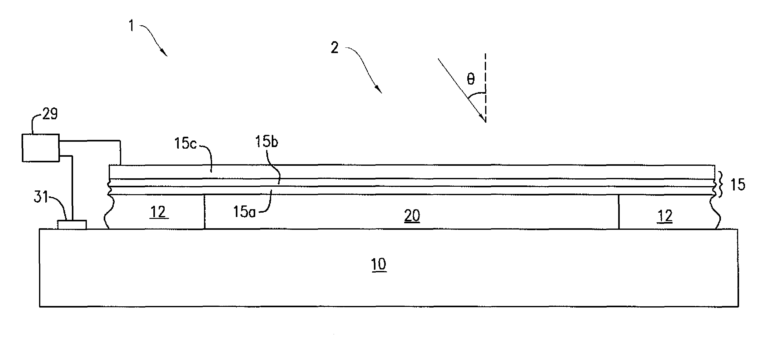
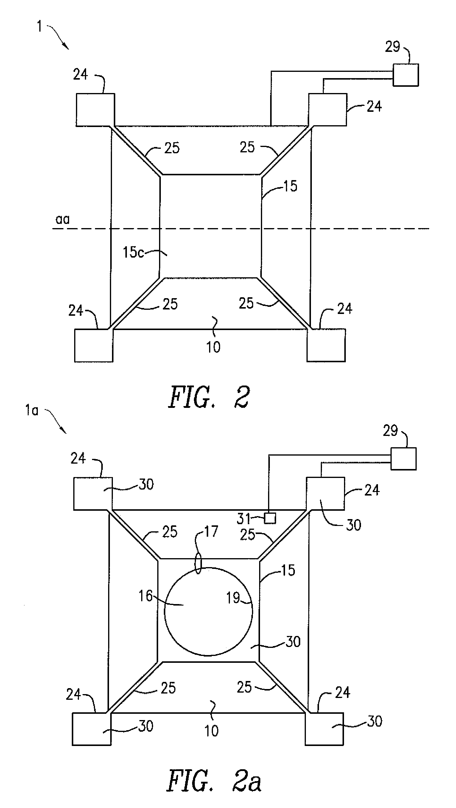
[0040]The present invention provides an apparatus for modulating an optical signal, and a method for its fabrication. The apparatus, which may be formed on a semiconductor wafer or chip, comprises a membrane and a substrate spaced to form an air gap. The membrane consists of three or more layers suspended over the substrate by support arms. There is a specific relationship between the refractive indices of the membrane layers and the refractive index of the substrate, and the membrane layers have specific thickness. A bias voltage is applied to the membrane and the substrate to generate an electrostatic force to move the membrane towards the substrate.

[0041]When the air gap is in the unbiased state, the membrane and air gap function as a high reflectivity coating. When the air gap is in the biased state, the membrane and air gap function as an anti-reflection coating. The membrane's change in reflectivity facilitates modulating the optical signal. In a preferred embodiment, the memb...


PUM


Abstract

A modulator for modulating an optical signal is disclosed having a substrate, a support mounted to the substrate, and membrane attached to the support and defining an airgap between the substrate and the membrane. The membrane has at least three layers including a central layer having an index of refraction which is the square root of the index of refraction of the substrate. The thickness of the layers and the size of the airgap are optimized to maximize differential reflectivity of light incident on the membrane at a non-normal angle of incidence to the membrane when the membrane is either in an unbiased state or biased state. In one embodiment, the first, central, and third layers have corresponding thicknesses approximately equal to one-quarter, one-quarter, and on-half of a wavelength of the optical signal, respectively. In another embodiment, the thickness of the layers and the airgap are designed according to formulas such that the modulator can operate over wider angles of incidence up to about 55 degrees. In a third embodiment, the modulator can operate at an angle of incidence-up to about 85 degree with TE-only polarization of the incident light.

Description

CROSS-REFERENCE TO RELATED APPLICATIONS[0001]This application claims the benefit of U.S. provisional patent application No. 60 / 659,750 filed Mar. 8, 2005, the disclosure of which is incorporated herein by reference in its entirety.RELATED FEDERALLY SPONSORED RESEARCH[0002]The work described in this application was sponsored by the Office of Naval Research under Contract Number N000140310490.FIELD OF THE INVENTION[0003]The present invention relates to optical modulators, and more particularly to micro-mechanical optical modulators that provide effective modulation over a wide angle-of-incidence.BACKGROUND OF THE INVENTION[0004]Inexpensive light modulators that have high contrast and wide optical bandwidths have been used in optical wavelength-division-multiplexing networks. A modulation device particularly well suited for the above application is a surface normal mechanically-active an-reflection switch (MARS) modulator. This device may be described as having a variable air gap defin...

Claims


Application Information

Patent Timeline
Patent Type & Authority Patents(United States)
IPC IPC(8): G02F1/03
CPCG02B26/001
Inventor GOOSSEN, KEITH
Owner DELAWARE UNIV OF A DE
Why Eureka
Try Eureka