Transfer pulse generator circuit and image pickup apparatus

a generator circuit and pulse technology, applied in the direction of pulse technique, generating/distributing signals, instruments, etc., can solve the problems of increased calorific power, increased power consumption, and high cost of the substrate formed with a ccd-type solid-state image pickup device, so as to mitigate visual recognition of image noise and hard visual recognition

Inactive Publication Date: 2010-06-15
SONY CORP
View PDF6 Cites 3 Cited by
  • Summary
  • Abstract
  • Description
  • Claims
  • Application Information

AI Technical Summary

Benefits of technology

[0026]The transfer pulse control means for controlling to set rise and fall timings of the vertical register transfer pulse to desired timings in a predetermined period can make the rise and fall timings of the vertical register transfer pulse different at each horizontal line so that timings of switching noises can be made different at each horizontal line. By making the timing of a potential change of a substrate formed with a CCD type solid state image pickup device different at each horizontal line, it is possible to make hard to visually recognize linear image noises in a vertical direction. Similarly, it is possible to make hard to visually recognize spot image noises on a screen, by making the rise and fall timings of the vertical register transfer pulse different at each field and / or frame.
[0033]The second predetermined value is set to an output value of the random number generator circuit for outputting a desired value in the predetermined period. It is therefore possible to make the rise and fall timings of the vertical register transfer pulse different at each horizontal line and make the timings of switching noises different at each horizontal line. Therefore, it is possible to make the timing of a potential change of the substrate formed with a CCD type solid state image pickup device different at each horizontal line. By making the timing of a potential change of the substrate formed with a CCD type solid state image pickup device different at each horizontal line, it becomes possible to make hard to visually recognize linear image noises in the vertical direction. The “predetermined period” means a period while the vertical register transfer pulse can be generated in the period while the vertical register transfer is not adversely affected. Namely, this period means a period while the vertical register transfer pulse can be generated which does not adversely affect the vertical register transfer by using as a trigger the reference signal output from the second comparator, even if the second predetermined value to be compared with the count of the second counter by the second comparator is changed.
[0034]With the transfer pulse generator circuit and image pickup apparatus of the present invention described above, it is possible to mitigate visual recognition of image noises on a screen of a video even if a vertical register transfer is performed in an effective pixel period.

Problems solved by technology

However, if a frame rate near a conventional frame rate is realized by raising the drive frequency at which a CCD type solid state image pickup device is driven, a rise in the drive frequency may cause an increase in a calorific power, an increase in a power consumption, high cost of a substrate formed with a CCD type solid state image pickup device, an increase in the number of peripheral components and the like.
It is therefore difficult to say that the method of raising a drive frequency at which a CCD type solid state image pickup device is driven, to realize a frame rate near a conventional frame rate, is proper.
Further, if only the countermeasure of raising the drive frequency is used, a limit is approaching for the recent requirements for improving the frame rate.
If a frame rate near a conventional frame rate is realized by performing a vertical register transfer during an effective pixel period, there arises, as described earlier, adverse influence of switching noises of vertical register transfer pulses.
Namely, a potential of a substrate formed with a CCD type solid state image pickup device changes at rise / fall timings of each vertical register transfer pulse, so that an output of the output circuit may be adversely affected and fixed pattern noises (FPN) may be generated.

Method used


Image

  • Transfer pulse generator circuit and image pickup apparatus
  • Transfer pulse generator circuit and image pickup apparatus
  • Transfer pulse generator circuit and image pickup apparatus

Examples


Embodiment Construction

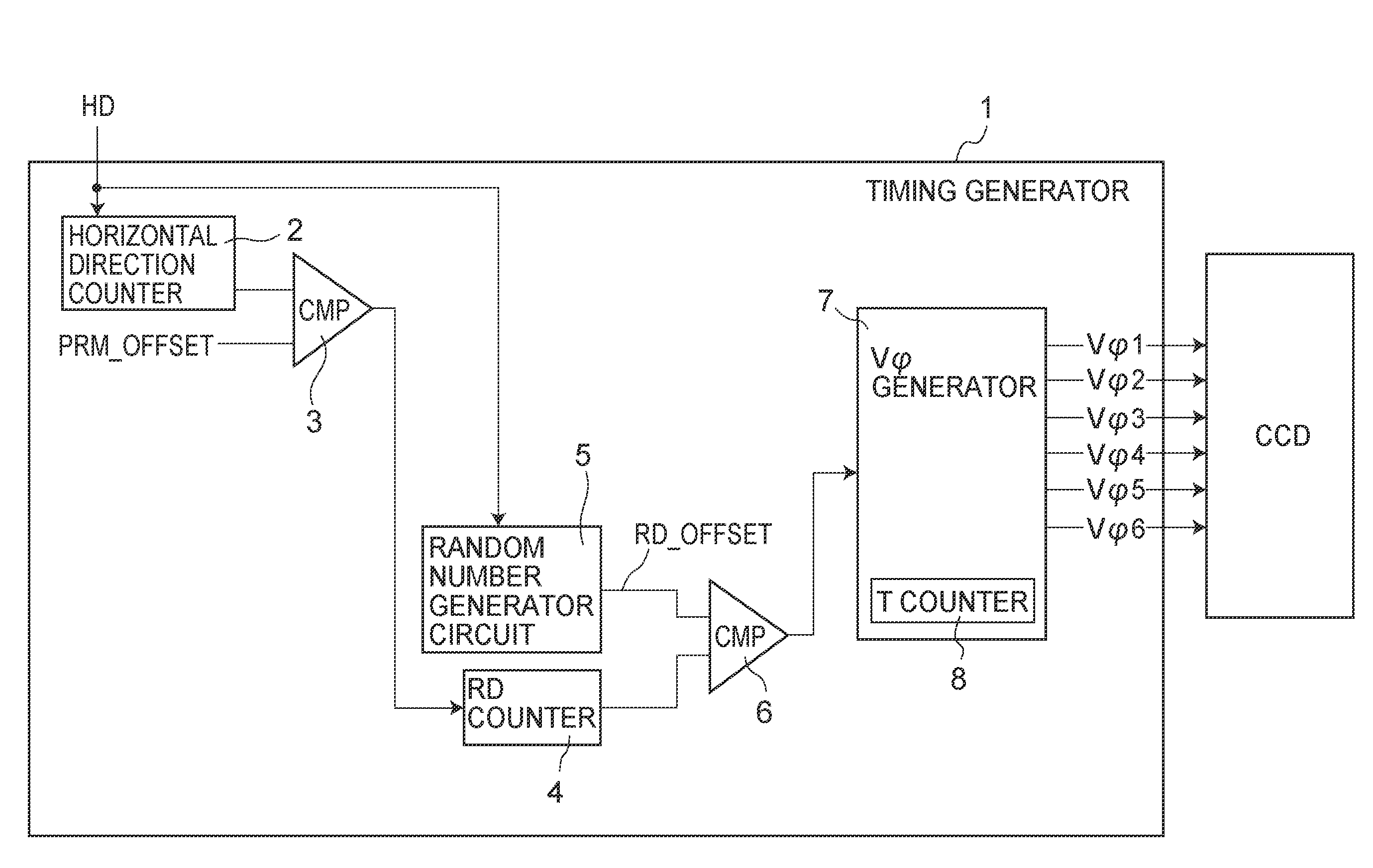
[0052]In the embodiments to be described hereunder, description will be made on the generation of basic timings by illustratively using pulses Vφ1 to Vφ6 similar to those shown in the timing charts of FIGS. 5 and 8. A rise timing of the pulse Vφ6 is T1, a fall timing of the pulse Vφ2 is T2, a rise timing of the pulse Vφ1 is T3, a fall timing of the pulse Vφ3 is T4, a rise timing of the pulse Vφ2 is T5, a fall timing of the pulse Vφ4 is T6, a rise timing of the pulse Vφ3 is T7, a fall timing of the pulse Vφ5 is T8, a rise timing of the pulse Vφ4 is T9, a fall timing of the pulse Vφ6 is T10, a rise timing of the pulse Vφ5 is T11, and a fall timing of the pulse Vφ1 is T12.

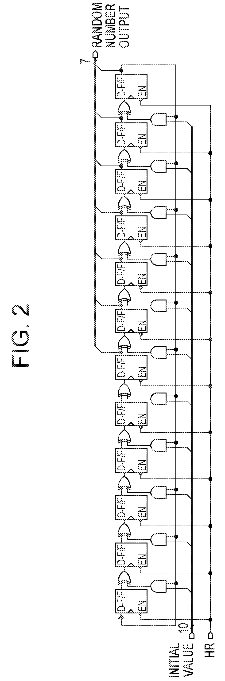
[0053]FIG. 1 is a schematic diagram showing a timing generator equipped with an example of a transfer pulse generator circuit applying the present invention. A timing generator 1 shown in the drawing is constituted of: a horizontal direction counter 2 which starts counting synchronously with a fall of a horizontal syn...


PUM


Abstract

A transfer pulse generator circuit for outputting a vertical register transfer pulse includes transfer pulse control means for controlling to set rise and fall timings of the vertical register transfer pulse to desired timings in a predetermined period.

Description

CROSS REFERENCES TO RELATED APPLICATIONS[0001]The present application contains subject matter related to Japanese Patent Application JP 2006-006652 filed in the Japanese Patent Office on Jan. 13, 2006 and JP 2006-283535 filed in the Japanese Patent Office on Oct. 18, 2006, the entire contents both of which being incorporated herein by reference.BACKGROUND OF THE INVENTION[0002]1. Field of the Invention[0003]The present invention relates to a transfer pulse generator circuit and an image pickup apparatus. More particularly, the present invention relates to a transfer pulse generator circuit for generating vertical register transfer pulses for driving vertical registers of a charge coupled device (CCD) type solid state image pickup device, and an image pickup apparatus equipped with a CCD type solid state image pickup device having the transfer pulse generator circuit.[0004]2. Description of Related Art[0005]In an image pickup apparatus equipped with a CCD type solid state image picku...

Claims


Application Information

Patent Timeline
Patent Type & Authority Patents(United States)
IPC IPC(8): H04N3/14H04N5/335H04N5/341H04N5/372H04N5/376
CPCH03K3/84H03K7/04H04N5/3765H04N3/155H04N5/3577H04N3/1537H04N25/617H04N25/73H04N25/745B65F1/1623B65D25/00B65D43/16B65F2001/1669
Inventor SHIMONO, TAKASHITAGAMI, HIROYASU
Owner SONY CORP
Why Eureka
Try Eureka