Eureka AIR delivers breakthrough ideas for toughest innovation challenges, trusted by R&D personnel around the world.

Ultra-fine area array pitch probe card

a probe card and ultra-fine area technology, applied in the field of ultra-fine area array pitch probe cards, can solve the problems of limited type of probe cards, inability to reach contact pads, and historically limited minimum pitch (the distance between electrical connections) of this type of cards, so as to reduce the pitch of the probe pins

Inactive Publication Date: 2010-06-08
TAIWAN SEMICON MFG CO LTD
View PDF23 Cites 18 Cited by
  • Summary
  • Abstract
  • Description
  • Claims
  • Application Information

AI Technical Summary

Benefits of technology

[0006]These and other problems are generally solved or circumvented, and technical advantages are generally achieved, by embodiments of the present invention that include a semiconductor device test structure. An advantage of embodiments of the present invention is that a smaller contact pitch can be obtained. This allows for the testing of smaller structures.
[0010]An advantage of a preferred embodiment of the present invention is that the pitch of the probe pins can be reduced in devices that incorporate the present invention. This invention allows these devices to test smaller devices than similar devices that do not incorporate this invention.

Problems solved by technology

Unfortunately, this type of probe card is limited due to the fact that the contact pads are limited to the peripheral of the semiconductor device to be tested, and cannot reach contact pads located in the central areas of the devices.
However, the minimum pitch (the distance between the electrical connections) for this type of card has historically been limited by the structure and shape of the electrical connections between the printed circuit board and the tips of the probe pins.
Unfortunately, as the dimensions of semiconductor devices are reduced in the ever-present drive for smaller and smaller devices, the pitches of these types of probe cards will be unable to adequately test semiconductor devices requiring a smaller probe pitch.

Method used


Image

  • Ultra-fine area array pitch probe card
  • Ultra-fine area array pitch probe card
  • Ultra-fine area array pitch probe card

Examples


Embodiment Construction

[0019]The making and using of the presently preferred embodiments are discussed in detail below. It should be appreciated, however, that the present invention provides many applicable inventive concepts that can be embodied in a wide variety of specific contexts. The specific embodiments discussed are merely illustrative of specific ways to make and use the invention, and do not limit the scope of the invention.

[0020]The present invention will be described with respect to embodiments in a specific context, namely a probe card. The invention may also be applied, however, to other non-permanent electrical connections.

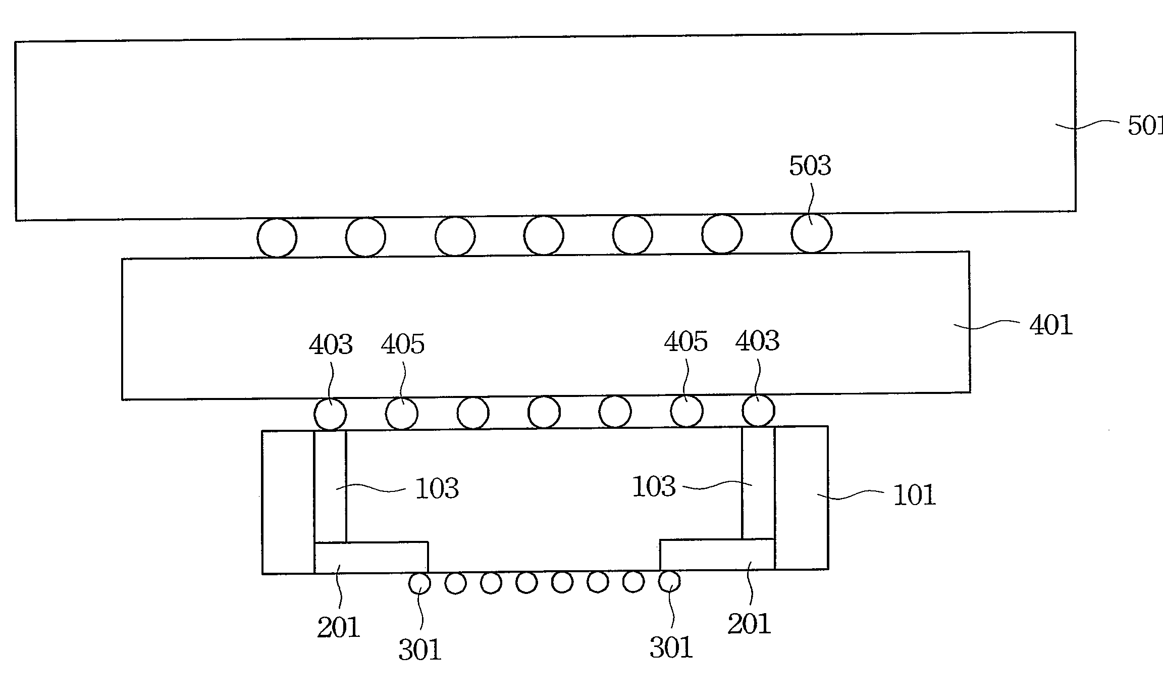
[0021]With reference now to FIG. 1, there is shown a silicon substrate 101 with vias 103 formed therein. The substrate 101 comprises a semiconductor material such as silicon, germanium, silicon germanium, or combinations thereof. The substrate 101 is initially between about 150 μm to about 762 μm, with a preferred thickness of about 500 μm.

[0022]The vias 103 preferably ex...


PUM


Abstract

A system and a method of testing a semiconductor die is provided. An embodiment includes a printed circuit board connected to a space transformation layer, which is connected to a substrate. The substrate uses through silicon vias and a redistribution layer to reduce the pitch of the connections beyond the historical limitations. A probe head using Cobra-style probe pins is connected to the redistribution layer through C4 bumps.

Description

TECHNICAL FIELD[0001]The present invention relates generally to a system for testing semiconductor devices and, more particularly, to a system and method for forming a probe card with an ultra-fine pitch.BACKGROUND[0002]In the manufacturing of integrated circuits and other semiconductor devices, the circuits and devices must be tested in order to ensure that a functional device has been manufactured. These tests are usually performed by contacting a test probe card to the relevant areas of the semiconductor device, sending current to the semiconductor device and performing one or more functional tests. Two main types of probe cards are currently used to make these connections.[0003]The first main type of probe card uses a series of cantilever connectors that radiate inward from the edges of the probe card. When the probe card is lowered onto the semiconductor device to be tested, the cantilevered connectors connect to corresponding contact pads on the semiconductor device to complet...

Claims


Application Information

Patent Timeline
Patent Type & Authority Patents(United States)
IPC IPC(8): G01R31/02
CPCG01R1/06744G01R1/07378G01R1/07357
Inventor CHENG, HSU MING
Owner TAIWAN SEMICON MFG CO LTD
Why Eureka
Eureka Blog
Learn More