Method and apparatus for maintaining data density for derived clocking
a clocking and data density technology, applied in the field of memory systems and components, can solve the problems of stub bus topology, difficult to achieve the next significant level, 800 megatransfer/second (mt/s) and beyond,
- Summary
- Abstract
- Description
- Claims
- Application Information
AI Technical Summary
Benefits of technology
Problems solved by technology
Method used
Image
Examples
Embodiment Construction
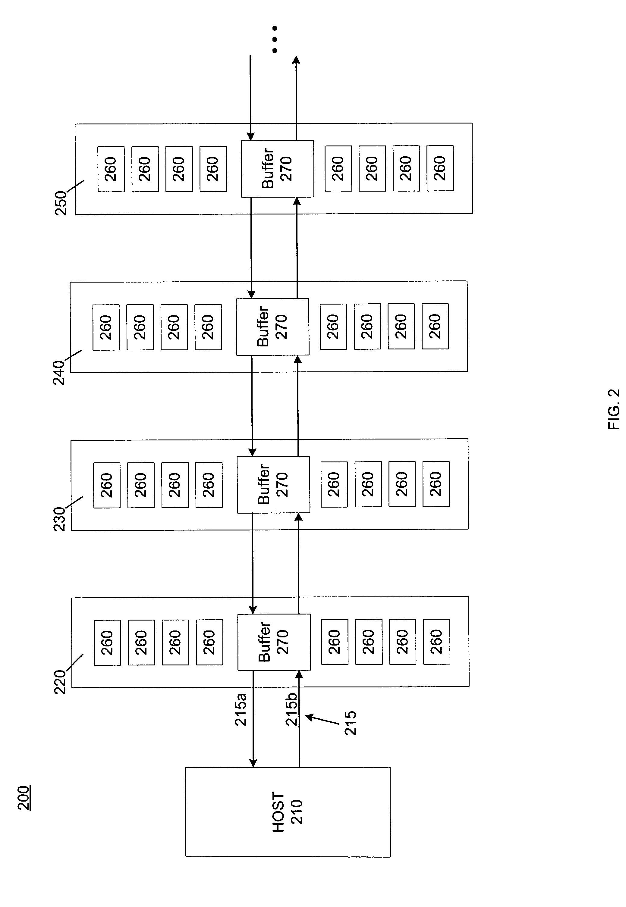
[0014]In order to increase memory bandwidth requirements above 4.2-5.3 GB / s per memory channel, embodiments of the invention utilize a “point-to-point” (P2P) signaling technology. FIG. 2 is a block diagram illustrating a memory channel 200 with a P2P topology. The P2P memory channel 200 includes four DIMMs 220, 230, 240, and 250. Each of the DIMMs has eight dynamic random access memory (DRAM) devices 260. Other P2P memory channels may have more or less DIMMs, but they will nonetheless still be arranged as illustrated in FIG. 2.
[0015]The host 210 and DIMMs 220-250 are connected to a memory bus 215, where 215a represents the inbound data stream (to the host) and 215b represents the outbound data stream (from the host). In this case, the inbound data path and the outbound data path from the DIMM 250 that is furthest from the host 210 is not used, since DIMM 250 is the last in the chain.
[0016]The host 210 can include one or more microprocessors, signal processors, memory controllers, gr...
PUM
 Abstract
Description
Claims
Application Information
 - R&D
- Intellectual Property
- Life Sciences
- Materials
- Tech Scout
- Unparalleled Data Quality
- Higher Quality Content
- 60% Fewer Hallucinations
Browse by: Latest US Patents, China's latest patents, Technical Efficacy Thesaurus, Application Domain, Technology Topic, Popular Technical Reports.
© 2025 PatSnap. All rights reserved.Legal|Privacy policy|Modern Slavery Act Transparency Statement|Sitemap|About US| Contact US: help@patsnap.com


