Optical module and processing method
a processing method and optical module technology, applied in the field of optical modules and processing methods, can solve the problems of difficult to effectively cut off large damage to other optical parts by the transmitting pumping light, and small output when being outputted from the connector. , to achieve the effect of high power, large damage to other optical parts, and large outpu
- Summary
- Abstract
- Description
- Claims
- Application Information
AI Technical Summary
Benefits of technology
Problems solved by technology
Method used
Image
Examples
first embodiment
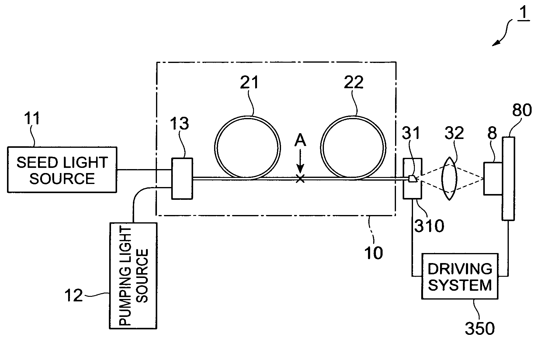
[0040]Next, a first embodiment of the optical module and processing method according to the present invention will be described. FIG. 4 is a view showing a structure of the first embodiment of the optical module according to the present invention. In FIG. 4, an optical module 1 according to the first embodiment is an optical device for processing a target to be processed 8. The module 1 includes the seed light source 11, the pumping light source 12, the optical coupler 13, an amplification optical fiber 21, an absorption optical fiber 22 which is fusion-spliced to the amplification optical fiber 21 at a connection point A, an APC optical connector 31 and an optical system 32. Further, a fiber unit 10 is constituted by the optical coupler 13, the amplification optical fiber 21, and the absorption optical fiber 22. Relative position adjustment of the target to be processed 8 relative to the APC optical connector 31 from which the amplified light is outputted is performed by moving a s...
second embodiment
[0054]Next, a second embodiment of the optical module and processing method according to the present invention will be described. FIG. 9 is a view showing a structure of the second embodiment of the optical module according to the present invention. In FIG. 9, an optical module 2 according to the second embodiment is an optical device for processing the target to be processed 8. The module 2 includes the seed light source 11, the pumping light source 12, the optical coupler 13, the amplification optical fiber 21, the absorption optical fiber 22 which is fusion-spliced to the amplification optical fiber 21 at the connection point A, a single-mode optical fiber 23, the APC optical connector 31 and the optical system 32. Further, a fiber unit 20 is constituted by the optical coupler 13, the amplification optical fiber 21, the absorption optical fiber 22, and the single-mode optical fiber 23. The relative position adjustment of the target to be processed 8 relative to the APC optical co...
third embodiment
[0061]Next, a third embodiment of the optical module and processing method according to the present invention will be described. FIG. 10 is a view showing a structure of the third embodiment of the optical module according to the present invention. An optical module 3 shown in FIG. 10 is an optical device for processing the target to be processed 8. The module 3 includes the seed light source 11, the pumping light source 12, the optical coupler 13, the amplification optical fiber 21, the absorption optical fiber 22, the single-mode optical fiber 23, the APC optical connector 31, and the optical system 32. Further, a fiber unit 30 is constituted by the optical coupler 13, the amplification optical fiber 21, the absorption optical fiber 22, and the single-mode optical fiber 23.
[0062]As compared to a structure of the optical module 2 according to the second embodiment shown in FIG. 9, the optical module 3 according to the third embodiment shown in FIG. 10 differs from the optical modul...
PUM
 Abstract
Description
Claims
Application Information
 - R&D
- Intellectual Property
- Life Sciences
- Materials
- Tech Scout
- Unparalleled Data Quality
- Higher Quality Content
- 60% Fewer Hallucinations
Browse by: Latest US Patents, China's latest patents, Technical Efficacy Thesaurus, Application Domain, Technology Topic, Popular Technical Reports.
© 2025 PatSnap. All rights reserved.Legal|Privacy policy|Modern Slavery Act Transparency Statement|Sitemap|About US| Contact US: help@patsnap.com


