Low power Bandgap reference circuit with increased accuracy and reduced area consumption
a reference circuit and low power bandgap technology, applied in the field of low power bandgap reference circuits, can solve the problems of reducing accuracy and often adverse effects of circuits including such devices, and achieve the effects of reducing mismatch-induced voltage offsets, reducing any mismatch-induced voltage offsets, and reducing the voltage offsets occurring within the operational amplifier
- Summary
- Abstract
- Description
- Claims
- Application Information
AI Technical Summary
Benefits of technology
Problems solved by technology
Method used
Image

Examples
Embodiment Construction
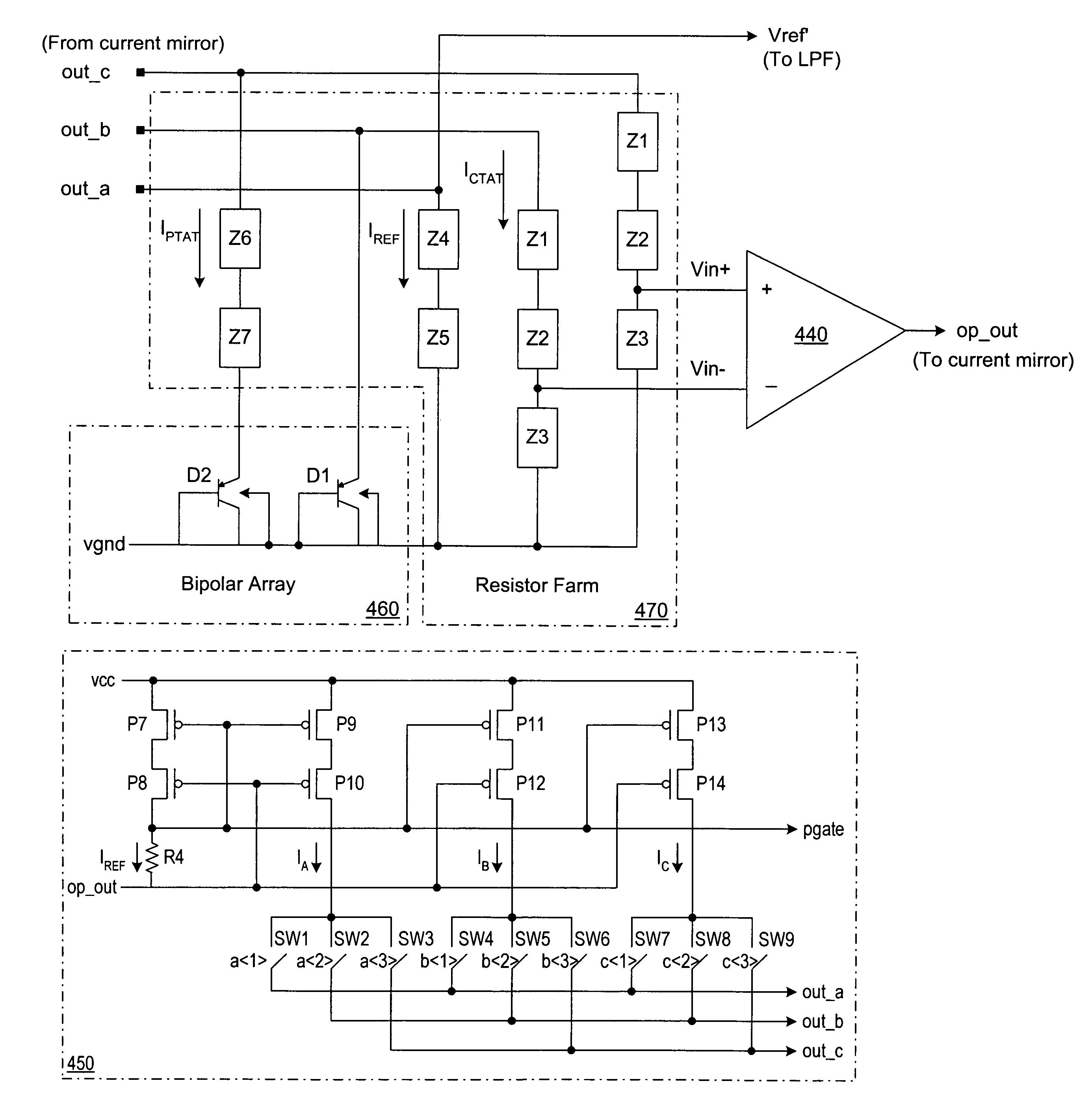
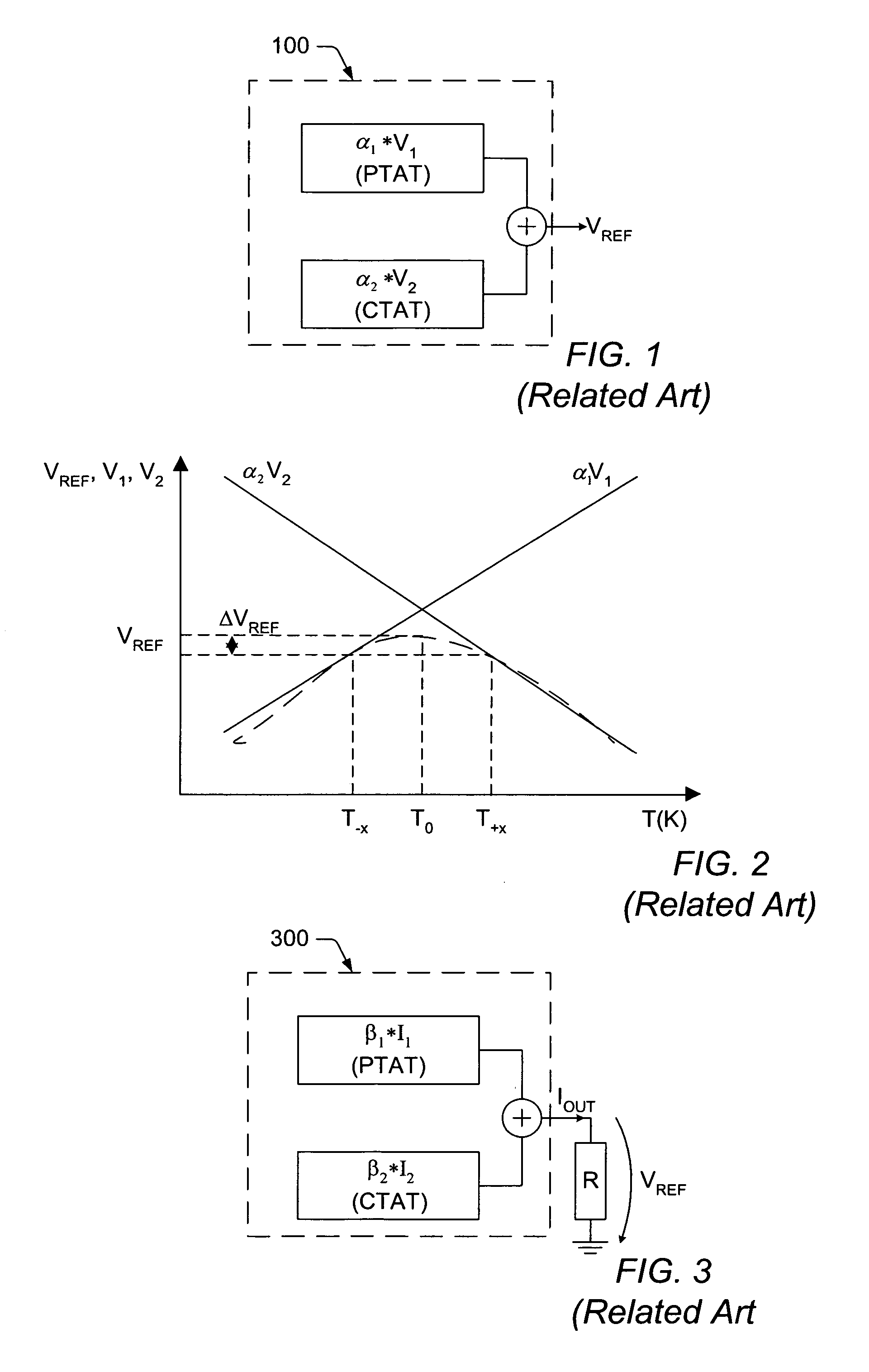
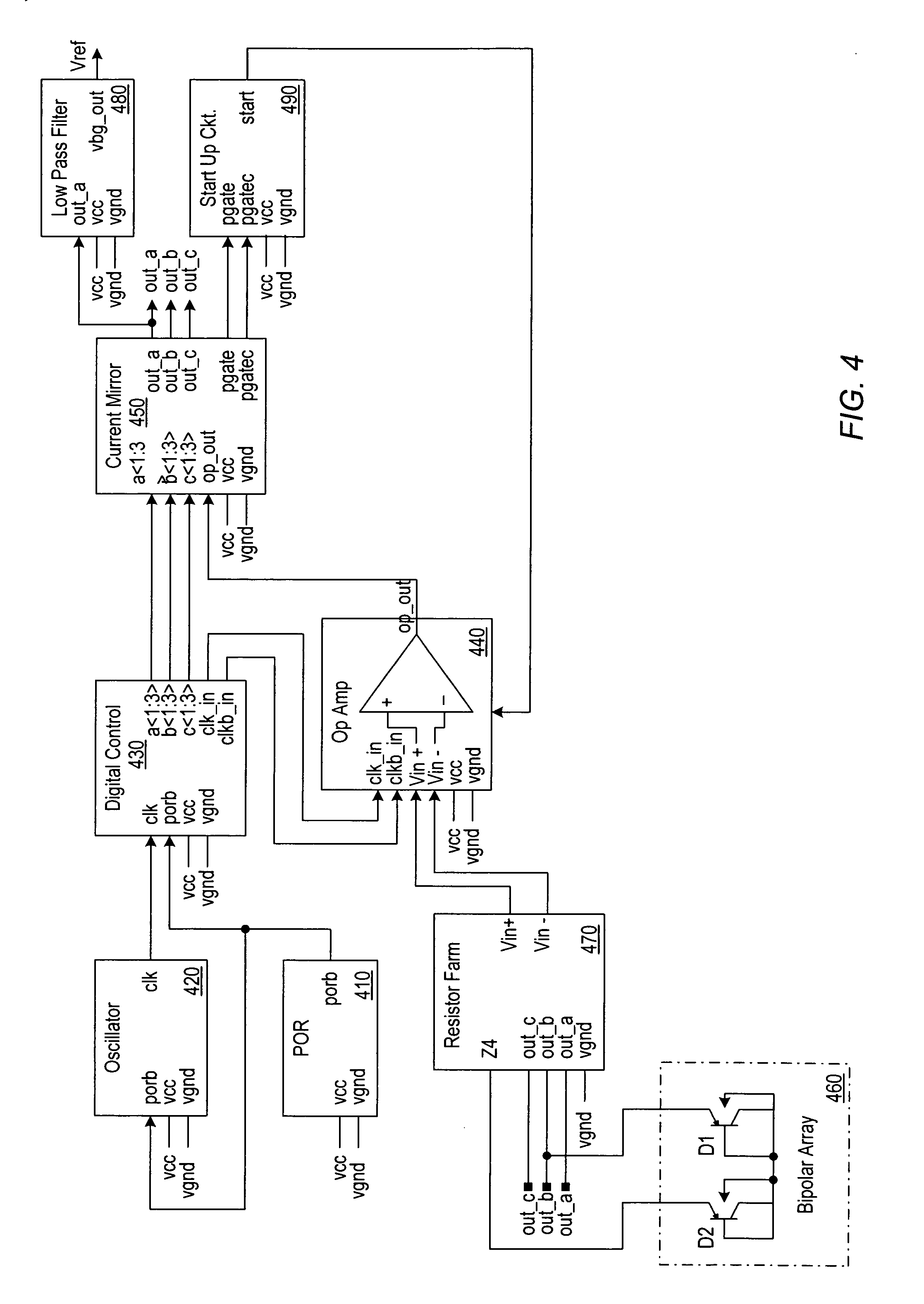
[0040]Bandgap reference (BGR) circuits are used for generating reference voltages, which exhibit relatively little variation across a defined range of temperatures, process corners and supply voltages. The two types of BGR circuits include voltage adding and current adding configurations. Although voltage adding BGR circuits are often successfully used for generating a single reference voltage output (e.g., about 1.25 volts) when supplied with a few volts (e.g., about 3 to 5 volts), they are generally unsuitable for low power operation (e.g., power supply voltages of about 1.6 volts and below) and applications, which prefer and / or require a different voltage output (e.g., other than 1.25 volts), multiple voltage outputs or a combination of voltage and current outputs.
[0041]For this reason, current adding BGR circuits are sometimes used to overcome the disadvantages of their voltage adding counterparts. However, in order to compensate for process-induced mismatch, most current adding...
PUM
 Abstract
Description
Claims
Application Information
 - R&D
- Intellectual Property
- Life Sciences
- Materials
- Tech Scout
- Unparalleled Data Quality
- Higher Quality Content
- 60% Fewer Hallucinations
Browse by: Latest US Patents, China's latest patents, Technical Efficacy Thesaurus, Application Domain, Technology Topic, Popular Technical Reports.
© 2025 PatSnap. All rights reserved.Legal|Privacy policy|Modern Slavery Act Transparency Statement|Sitemap|About US| Contact US: help@patsnap.com