Low noise amplifier

a low-noise amplifier and low-noise technology, applied in the field of amplifiers and circuits, can solve the problems of increasing the linearity requirement, the potential interference of an adjacent channel jammer, and the high noise level of broadband low-noise amplifiers

Inactive Publication Date: 2010-03-02
IND TECH RES INST
View PDF1 Cites 21 Cited by
  • Summary
  • Abstract
  • Description
  • Claims
  • Application Information

AI Technical Summary

Benefits of technology

[0009]Additional features and advantages of the invention will be set forth in the description that follows, being apparent from the description or learned by practice of embodiments of the invention. The features and other advantages of the invention will be realized and attained by the low-noise amplifier circuit designs pointed out in the written description and claims, as well as the appended drawings.
[0011]FIG. 1 shows a low-noise amplifier circuit consistent with embodiments of the invention;
[0012]FIG. 2A shows a low-noise amplifier circuit consistent with embodiments of the invention;
[0013]FIG. 2B shows a low-noise amplifier circuit consistent with embodiments of the invention;
[0014]FIG. 2C shows a low-noise amplifier circuit consistent with embodiments of the invention;
[0015]FIG. 3A shows a low-noise amplifier circuit consistent with embodiments of the invention;
[0016]FIG. 3B shows a low-noise amplifier circuit consistent with embodiments of the invention;
[0017]FIG. 3C shows a low-noise amplifier circuit consistent with embodiments of the invention;
[0018]FIG. 3D shows a low-noise amplifier circuit consistent with embodiments of the invention.
[0019]FIG. 4A shows a plot of voltage gain vs. input voltage frequency for a low-noise amplifier circuit configured as shown in FIG. 3A, utilizing dual cross-coupling technique;
[0020]FIG. 4B shows a plot of voltage gain vs. input voltage frequency for a low-noise amplifier circuit configured as shown in FIG. 3A, without utilizing dual cross-coupling;
[0021]FIG. 5A shows a plot of noise figure vs. input signal frequency for a low noise-amplifier circuit configured as shown in FIG. 3A, utilizing dual cross-coupling;
[0022]FIG. 5B shows a plot of noise figure vs. input signal frequency for a low noise-amplifier circuit configured as shown in FIG. 3A, without utilizing dual cross-coupling.
[0029]Common gate amplifier circuit 206 is cascode coupled to amplifier circuit 230 by coupling drain 216 of MOS transistor M1210 to source 238 of MOS transistor M3234. Common source amplifier circuit 208 is cascode coupled to amplifier circuit 232 by coupling drain 226 of MOS transistor M2220 to source 246 of MOS transistor M4242.
[0029]Common gate amplifier circuit 206 is cascode coupled to amplifier circuit 230 by coupling drain 216 of MOS transistor M1210 to source 238 of MOS transistor M3234. Common source amplifier circuit 208 is cascode coupled to amplifier circuit 232 by coupling drain 226 of MOS transistor M2220 to source 246 of MOS transistor M4242.
[0029]Common gate amplifier circuit 206 is cascode coupled to amplifier circuit 230 by coupling drain 216 of MOS transistor M1210 to source 238 of MOS transistor M3234. Common source amplifier circuit 208 is cascode coupled to amplifier circuit 232 by coupling drain 226 of MOS transistor M2220 to source 246 of MOS transistor M4242.
[0026]Amplifier circuit 206 includes an MOS transistor M1210 including a gate 212, a source 214, and a drain 216. Transistor M1210 also includes a substrate terminal 218. Amplifier circuit 208 includes an MOS transistor M2220, including a gate 222, a source 224, and a drain 226. Transistor M2220 also includes a substrate terminal 228.
[0027]Current buffer stage circuit204 includes an amplifier circuit 230 and an amplifier circuit 232. Amplifier circuit 230 includes an MOS transistor M3234 including a gate 236, a source 238, and drain 240. Amplifier circuit 232 includes an MOS transistor M4242 including a gate 244, a source 246, and a drain 248.
[0027]Current buffer stage circuit204 includes an amplifier circuit 230 and an amplifier circuit 232. Amplifier circuit 230 includes an MOS transistor M3234 including a gate 236, a source 238, and drain 240. Amplifier circuit 232 includes an MOS transistor M4242 including a gate 244, a source 246, and a drain 248.
[0027]Current buffer stage circuit204 includes an amplifier circuit 230 and an amplifier circuit 232. Amplifier circuit 230 includes an MOS transistor M3234 including a gate 236, a source 238, and drain 240. Amplifier circuit 232 includes an MOS transistor M4242 including a gate 244, a source 246, and a drain 248.
[0027]Current buffer stage circuit204 includes an amplifier circuit 230 and an amplifier circuit 232. Amplifier circuit 230 includes an MOS transistor M3234 including a gate 236, a source 238, and drain 240. Amplifier circuit 232 includes an MOS transistor M4242 including a gate 244, a source 246, and a drain 248.
[0027]Current buffer stage circuit204 includes an amplifier circuit 230 and an amplifier circuit 232. Amplifier circuit 230 includes an MOS transistor M3234 including a gate 236, a source 238, and drain 240. Amplifier circuit 232 includes an MOS transistor M4242 including a gate 244, a source 246, and a drain 248.
[0027]Current buffer stage circuit204 includes an amplifier circuit 230 and an amplifier circuit 232. Amplifier circuit 230 includes an MOS transistor M3234 including a gate 236, a source 238, and drain 240. Amplifier circuit 232 includes an MOS transistor M4242 including a gate 244, a source 246, and a drain 248.
[0026]Amplifier circuit 206 includes an MOS transistor M1210 including a gate 212, a source 214, and a drain 216. Transistor M1210 also includes a substrate terminal 218. Amplifier circuit 208 includes an MOS transistor M2220, including a gate 222, a source 224, and a drain 226. Transistor M2220 also includes a substrate terminal 228.
[0027]Current buffer stage circuit204 includes an amplifier circuit 230 and an amplifier circuit 232. Amplifier circuit 230 includes an MOS transistor M3234 including a gate 236, a source 238, and drain 240. Amplifier circuit 232 includes an MOS transistor M4242 including a gate 244, a source 246, and a drain 248.
[0027]Current buffer stage circuit204 includes an amplifier circuit 230 and an amplifier circuit 232. Amplifier circuit 230 includes an MOS transistor M3234 including a gate 236, a source 238, and drain 240. Amplifier circuit 232 includes an MOS transistor M4242 including a gate 244, a source 246, and a drain 248.

Problems solved by technology

These traditional broadband low-noise amplifiers generally have high noise levels as compared to inductive source degeneration low-noise amplifiers commonly used in narrowband systems.
Broadband communications present challenges for RF receiver design that are not presented by narrowband communications such as Global System for Mobile Communications (GSM) and Wideband Code Division Multiple Access (WBCDMA).
For example, an increased potential for interference from an adjacent channel jammer raises the linearity requirement.
So, multimedia wireless communications may present harsher design requirements, including broadband gain flatness, higher linearity requirements, and lower noise figures.
Thus, the circuit properties of low-noise amplifier circuits may directly impact the characteristics of the receiver as a whole.

Method used


Image

  • Low noise amplifier
  • Low noise amplifier
  • Low noise amplifier

Examples


Embodiment Construction

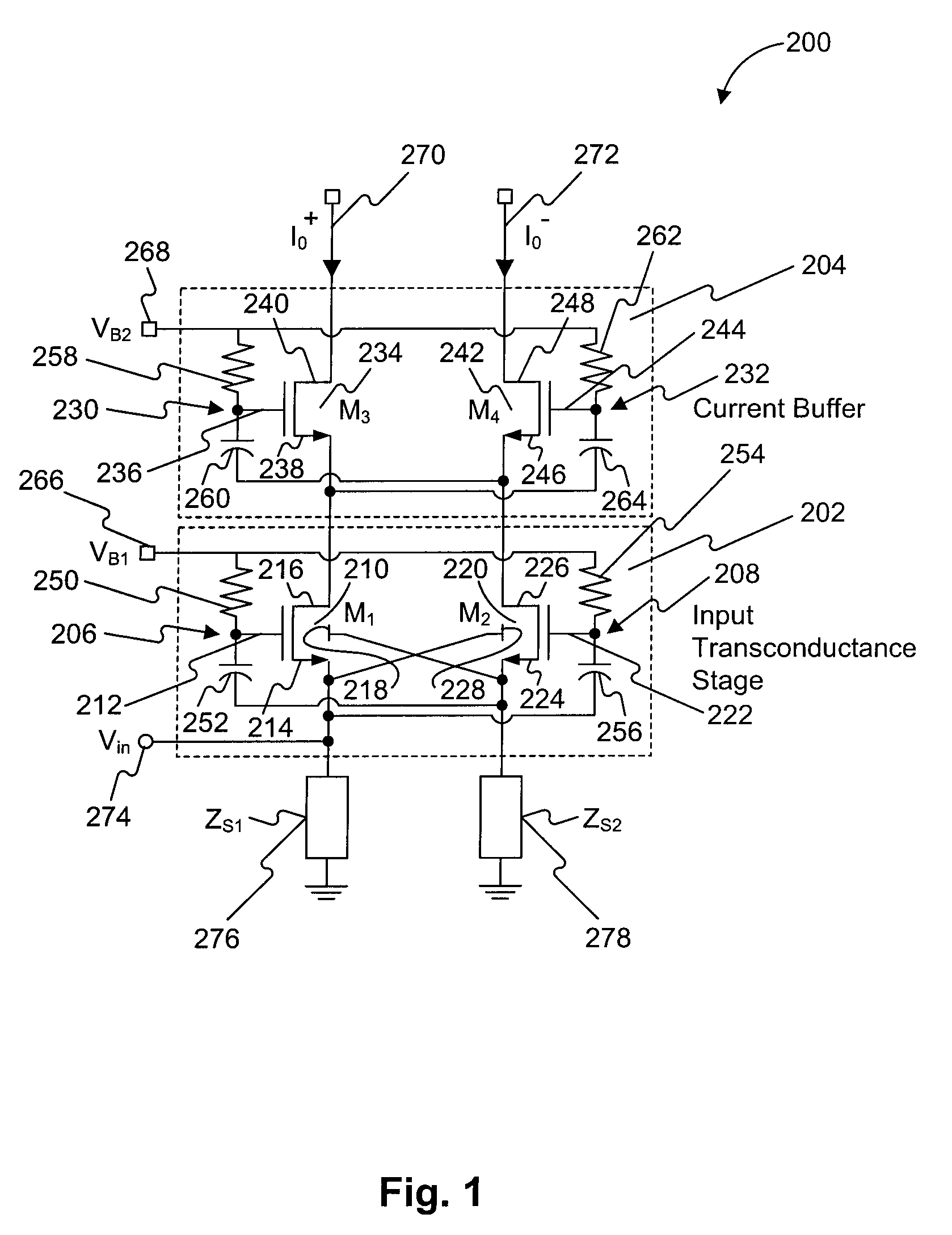
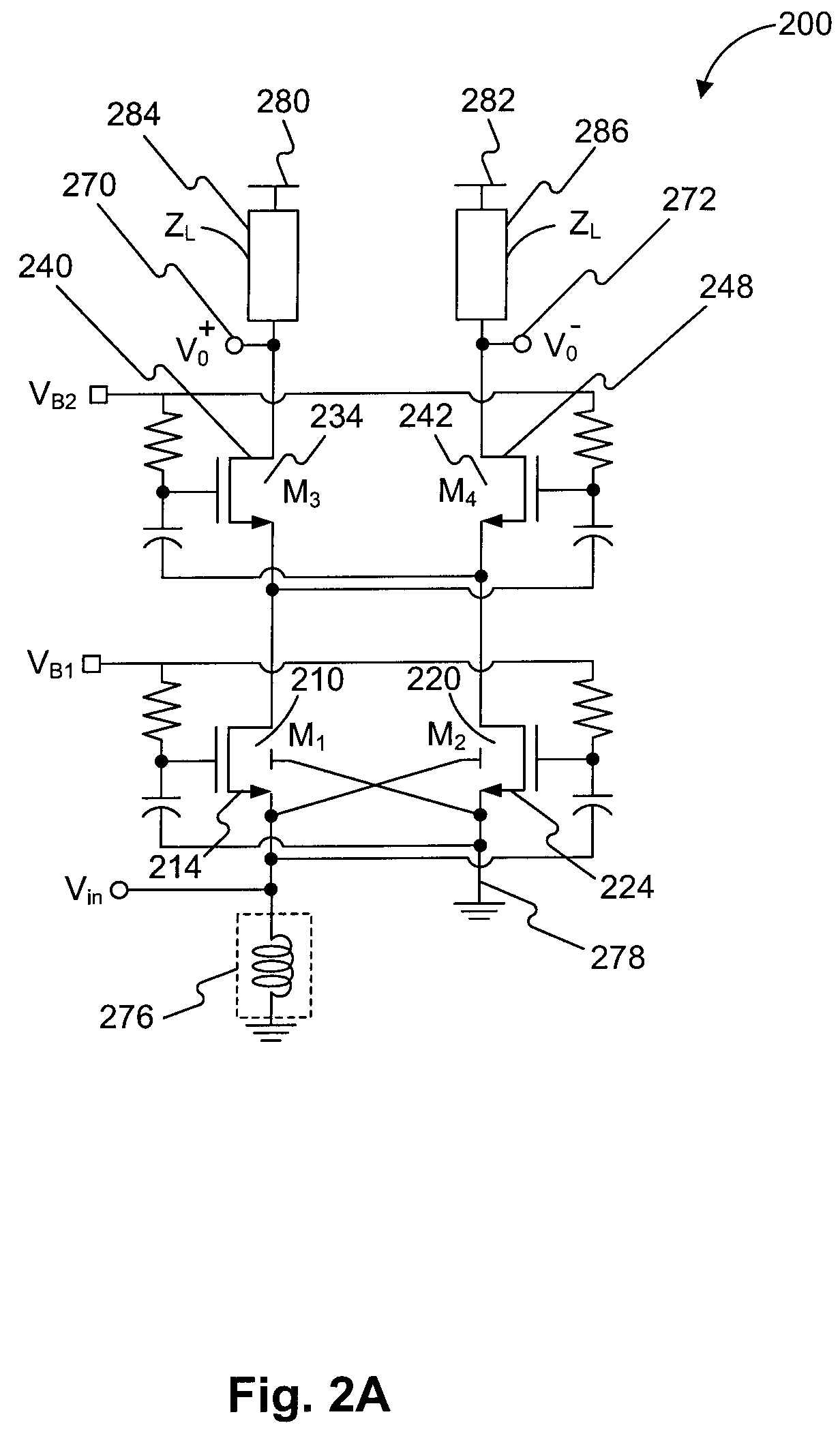
[0023]Reference will now be made in detail to exemplary embodiments, examples of which are illustrated in the accompanying drawings. The following description refers to the accompanying drawings in which the same numbers in different drawings represent the same or similar elements unless otherwise represented. The implementations set forth in the following description of exemplary embodiments consistent with the present invention do not represent all implementations consistent with the invention. Instead, they are merely examples of systems and methods consistent with aspects related to the invention as recited in the appended claims.

[0024]FIG. 1 shows a low-noise amplifier circuit 200 consistent with embodiments of the invention. Low-noise amplifier circuit 200 includes an input transconductance stage circuit 202 and a current buffer stage circuit 204, with input transconductance stage circuit 202 being cascode coupled to current buffer stage circuit 204, forming a cascode amplifie...


PUM


Abstract

A low-noise amplifier circuit to convert a single-ended input into a dual-ended output includes an input transconductance stage circuit, including a first MOS transistor coupled in parallel with a second MOS transistor; a current buffer circuit, including a third MOS transistor coupled in parallel with a fourth MOS transistor; each of the first, second, third, and fourth transistors having a body, gate, source, and drain; the input transconductance stage circuit and the current buffer circuit being cascode coupled, forming a cascode amplifier configuration; the single-ended input being at the source of one of the first and second transistors in the input transconductance stage circuit; the dual-ended output being a differential output across the drain of the third transistor and the drain of the fourth transistor; the first and second transistors of the input transconductance stage circuit being cross-coupled, wherein the body of the first transistor is coupled to the source of the second transistor, and the body of the second transistor is coupled to the source of the first transistor; and the third and fourth transistors of the current buffer circuit being cross-coupled, wherein a first capacitance is coupled between the gate of the third transistor and the source of the fourth transistor, and a second capacitance is coupled between the gate of the fourth transistor and the source of the third transistor.

Description

RELATED APPLICATIONS[0001]This application claims priority of U.S. Provisional Patent Application No. 60 / 960,988 filed Oct. 24, 2007, the contents of which are incorporated herein by reference. This application is related to application Ser. No. 12 / 188,276.FIELD OF THE INVENTION[0002]Systems, circuits, and methods disclosed herein relate to amplifiers, circuits and, more particularly, to low-noise amplifier circuits.DESCRIPTION OF THE RELATED ART[0003]Spectrums designated by new standards for wireless communications are becoming increasingly broad. For example, ultra-wide band technology (UWB) utilizes the 3.1˜10.6 GHz band range, where there is a triple highest / lowest band ratio; digital video broadcasting-handheld technology (DVB-H) utilizes the 474˜862 MHz band range, where there is a nearly double highest / lowest band ratio; and Digital Video Broadcasting-Terrestrial (DVB-T) technology utilizes the 50˜850 MHz band range, where there is a 17-fold highest / lowest band ratio.[0004]Fr...

Claims


Application Information

Patent Timeline
Patent Type & Authority Patents(United States)
IPC IPC(8): H03F3/04
CPCH03F3/19H03F3/45179H03F2200/294H03F2203/45306H03F2203/45318
Inventor KUO, MING-CHINGKAO, SHIAU-WENCHEN, CHIH-HUNG
Owner IND TECH RES INST
Why Eureka
Try Eureka