Memory device having implanted oxide to block electron drift, and method of manufacturing the same

a technology of flash memory and oxide, which is applied in the direction of semiconductor devices, basic electric elements, electrical equipment, etc., can solve the problems of affecting the memory window of the second bit, challenging obstacles, and disturbing the transitory program phenomenon

Inactive Publication Date: 2009-11-24
MONTEREY RES LLC
View PDF3 Cites 5 Cited by
  • Summary
  • Abstract
  • Description
  • Claims
  • Application Information

AI Technical Summary

Problems solved by technology

However, as the-above described cells are scaled smaller in size, a transient program disturb phenomenon becomes a challenging obstacle.
Transient program disturb results during programming of the dual bit devices.
This injection of secondary electrons into the charge trapping stack 18 may adversely affect the memory window of the second bit 30.

Method used


Image

  • Memory device having implanted oxide to block electron drift, and method of manufacturing the same
  • Memory device having implanted oxide to block electron drift, and method of manufacturing the same
  • Memory device having implanted oxide to block electron drift, and method of manufacturing the same

Examples


Embodiment Construction

[0013]The following detailed description of the invention is merely exemplary in nature and is not intended to limit the invention or the application and uses of the invention. Furthermore, there is no intention to be bound by any theory presented in the preceding background of the invention or the following detailed description of the invention.

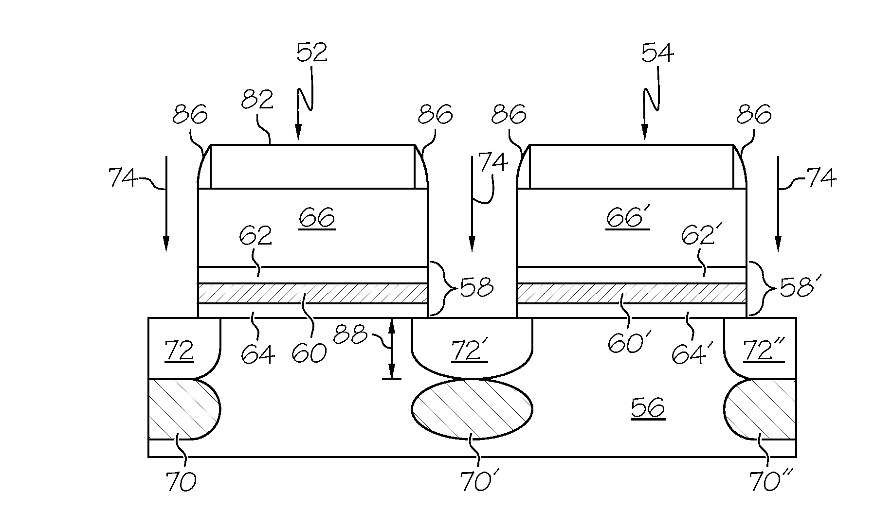
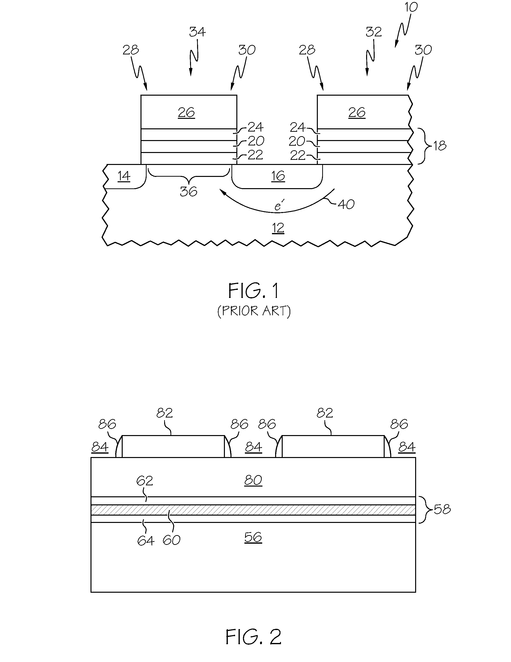
[0014]In accordance with an exemplary embodiment of the present invention, FIGS. 2 to 5 are cross-sectional views illustrating an exemplary method for fabricating a memory device, such as a dual bit memory device, that can be scaled with decreased device dimensions while overcoming challenges of transient program disturb. Various steps in the manufacture of a flash memory device are well known and so, in the interest of brevity, many conventional steps will only be mentioned briefly herein or will be omitted entirely without providing well known process details.

[0015]As illustrated in FIG. 2, an exemplary manufacturing process begins by prov...


PUM


Abstract

A memory device includes a substrate, a first gate stack overlying the substrate, a second gate stack overlying the substrate and spaced apart from the first gate stack, an oxide region formed at a first depth within the substrate and between the first and second gate stacks, and an impurity doped region formed at a second depth within the substrate and between the first and second gate stacks, the first depth being lower than the second depth.

Description

FIELD OF THE INVENTION[0001]The present invention generally relates to flash memory devices, and more particularly relates to methods for fabricating memory devices with reduced transient program disturb.BACKGROUND OF THE INVENTION[0002]A type of commercially available flash memory product is a MirrorBit® memory device available from Spansion, LLC. A MirrorBit® cell effectively doubles the intrinsic density of a flash memory array by storing two physically distinct bits on opposite sides of a memory cell. Each bit within a cell can be programmed with a binary unit of data (either a logic one or zero) that is mapped directly to the memory array.[0003]An exemplary MirrorBit® memory device 10, illustrated in FIG. 1, includes a P-type semiconductor substrate 12 within which is formed a plurality of spaced-apart source and drain regions 14 and 16, respectively, otherwise known as bit lines. Typically, the substrate 12 has P-type conductivity, and both of the bit lines 14 and 16 have N-ty...

Claims


Application Information

Patent Timeline
Patent Type & Authority Patents(United States)
IPC IPC(8): H01L21/425
CPCH01L29/792H01L21/7624
Inventor ZHENG, WEILEE, CHUNGHO
Owner MONTEREY RES LLC
Why Eureka
Try Eureka