
Apparatus, method, and system for flash memory

a technology of flash memory and apparatus, applied in the field of memory devices, can solve the problems of data corruption or loss, one or more threshold voltage states may be difficult to program properly than other states, and the memory cells will not properly represent the data intended to be stored into the memory cells

Active Publication Date: 2009-11-17
INTEL NDTM US LLC
View PDF7 Cites 57 Cited by
  • Summary
  • Abstract
  • Description
  • Claims
  • Application Information

AI Technical Summary

Benefits of technology

This approach minimizes the negative effects of program disturb and floating gate-to-floating gate interference, ensuring accurate data storage and retrieval by maintaining tight threshold voltage distributions, reducing data corruption, and improving programming speed and reliability.

Problems solved by technology

If the threshold voltages programmed into the memory cells are not in the intended range of threshold voltages, the memory cells will not properly represent the data that was intended to be stored into the memory cells.
In addition, even if the threshold voltage as originally programmed into the cells was within the proper range for the intended data, if the threshold voltage is not maintained within the proper range, the data stored in the memory cell will be corrupted or lost.
This may result in a problem wherein the threshold voltage of a cell first written into varies according to the data written into an adjacent cell.
In programming multiple level memory cells, one or more states for threshold voltages may be harder to properly program than other states.
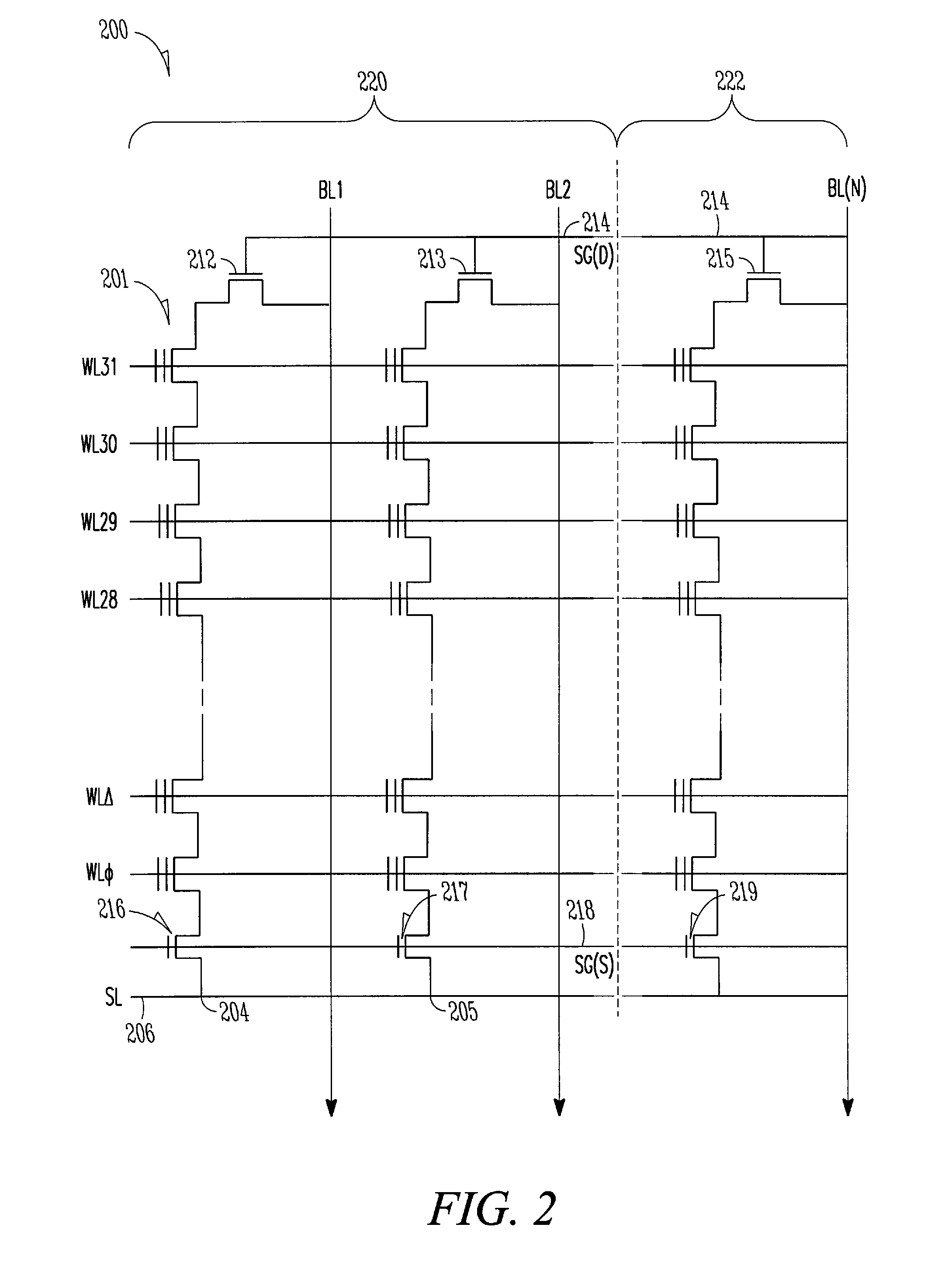
When one of these pages is being programmed, the second page on the same WL will experience a disturb condition even though it is inhibited.
Therefore pages with shared WLs can experience programming disturb.
This large voltage shift may create a FG-FG interference that may corrupt the data being programmed into one or more adjacent memory cells 501.
In general it is difficult to achieve a narrow threshold voltage distribution for a given group of memory cell when the threshold voltages are programmed from a wider threshold voltage distribution.

Method used


Image

  • Apparatus, method, and system for flash memory
  • Apparatus, method, and system for flash memory
  • Apparatus, method, and system for flash memory

Examples


Embodiment Construction

[0012]In a multiple level NAND flash memory cell, tight threshold voltage distribution is important. Tight control over programming refers to the ability to program threshold voltages in a multiple level memory cell within any one of designated ranges of threshold voltages so that the programmed threshold voltage properly represents the data intended to be stored in the multiple level memory cell.

[0013]For example, in a 4-bit per cell memory device wherein 4 bits of data may be stored in a single memory cell, 16 states are needed. Each state is generally represented by a defined range of threshold voltages that may be programmed into a multiple level memory cell in order to represent a particular state. If the threshold voltages programmed into the memory cells are not in the intended range of threshold voltages, the memory cells will not properly represent the data that was intended to be stored into the memory cells. In addition, even if the threshold voltage as originally program...


PUM


Abstract

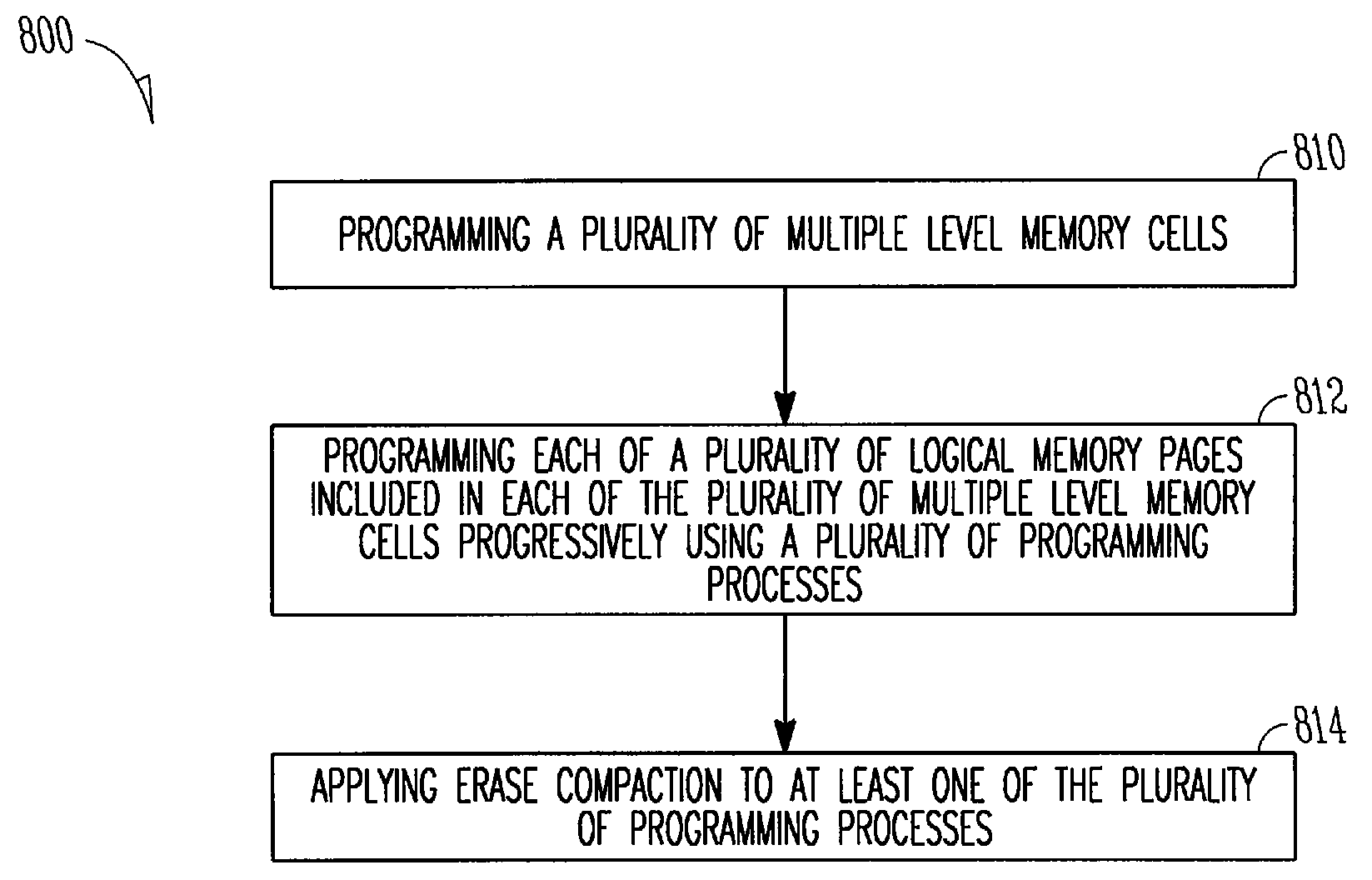
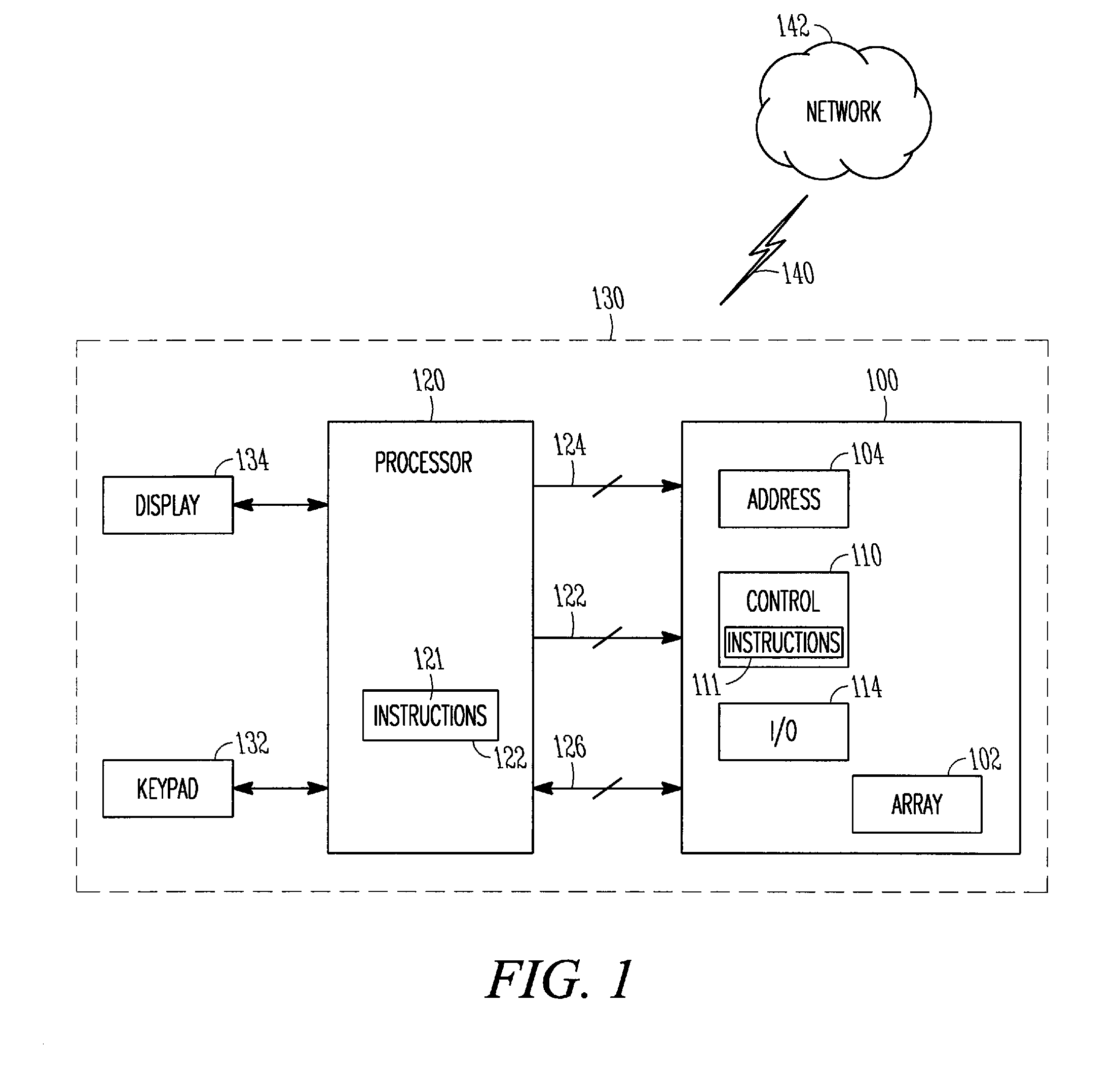
Methods, apparatus, systems, and data structures are disclosed, including a plurality of multiple level memory cells, each of the plurality of multiple level memory cells coupled to one of a plurality of wordlines and each of the plurality of multiple level memory cells including a plurality of logical memory pages; a control circuit coupled to the plurality of wordlines, the control circuit operable to progressively program each of the plurality of multiple level memory cells in at least one sequence including separation of the programming of a first logical memory page and a second logical memory page in any one of the plurality of multiple level memory cells by at least N−1 programming operations to memory cells either coupled to a different wordline or included in a different logical even page or a different logical odd page.

Description

TECHNICAL FIELD[0001]Various embodiments described herein relate generally to memory devices, including flash memory devices.BACKGROUND[0002]Memory devices can be categorized in two broad areas: volatile and non-volatile. Volatile memory devices require power to maintain data, while non volatile memories are capable of maintaining data in the absence of a power supply. An example of a non-volatile memory is the flash memory that stores information in a semiconductor device without the need for power being supplied to the semiconductor device in order to maintain the information in the semiconductor device.[0003]Flash memory may be built using either NOR or NAND devices. NAND flash may be either of single-level cell (SLC) or multiple-level cell (MLC) configuration. MLC NAND flash allows for a higher density memory device in comparison to SLC NAND flash because it allows the storage of two or more data bits in each memory cell.BRIEF DESCRIPTION OF THE DRAWINGS[0004]FIG. 1 illustrates ...

Claims


Application Information

Patent Timeline
Patent Type & Authority Patents(United States)
IPC IPC(8): G11C11/34
CPCG11C11/5628
Inventor ARITOME, SEIICHI
Owner INTEL NDTM US LLC
Learn More