Micro electronic component

a technology of electronic components and components, applied in the field of microelectronic components, can solve problems such as defective connections, and achieve the effect of simple bonding and simple design

Inactive Publication Date: 2009-10-13
UNIV DUISBURG ESSEN
View PDF25 Cites 1 Cited by
  • Summary
  • Abstract
  • Description
  • Claims
  • Application Information

AI Technical Summary

Benefits of technology

[0018]Preferably, the clusters are arranged essentially in lines or rows. According to a preferred embodiment, this is enabled very easily by housing the clusters in parallel grooves of equal size.
[0019]A very simple design and very simple bonding is preferably achieved by forming the first and second connecting electrodes in strips and arranging them such that the first connecting electrodes run parallel to each other and the second connecting electrodes run parallel to each other and crosswise to the first connecting electrodes, with a first and a second connecting electrode being in electrical contact with each other at their appropriate intersecting point preferably by means of a single cluster.

Problems solved by technology

Furthermore, there can also be defective connections in so far as two connecting electrodes contact two parallel, adjacent clusters instead of an in-between cluster at an intersecting point.

Method used


Image

  • Micro electronic component
  • Micro electronic component
  • Micro electronic component

Examples


first embodiment

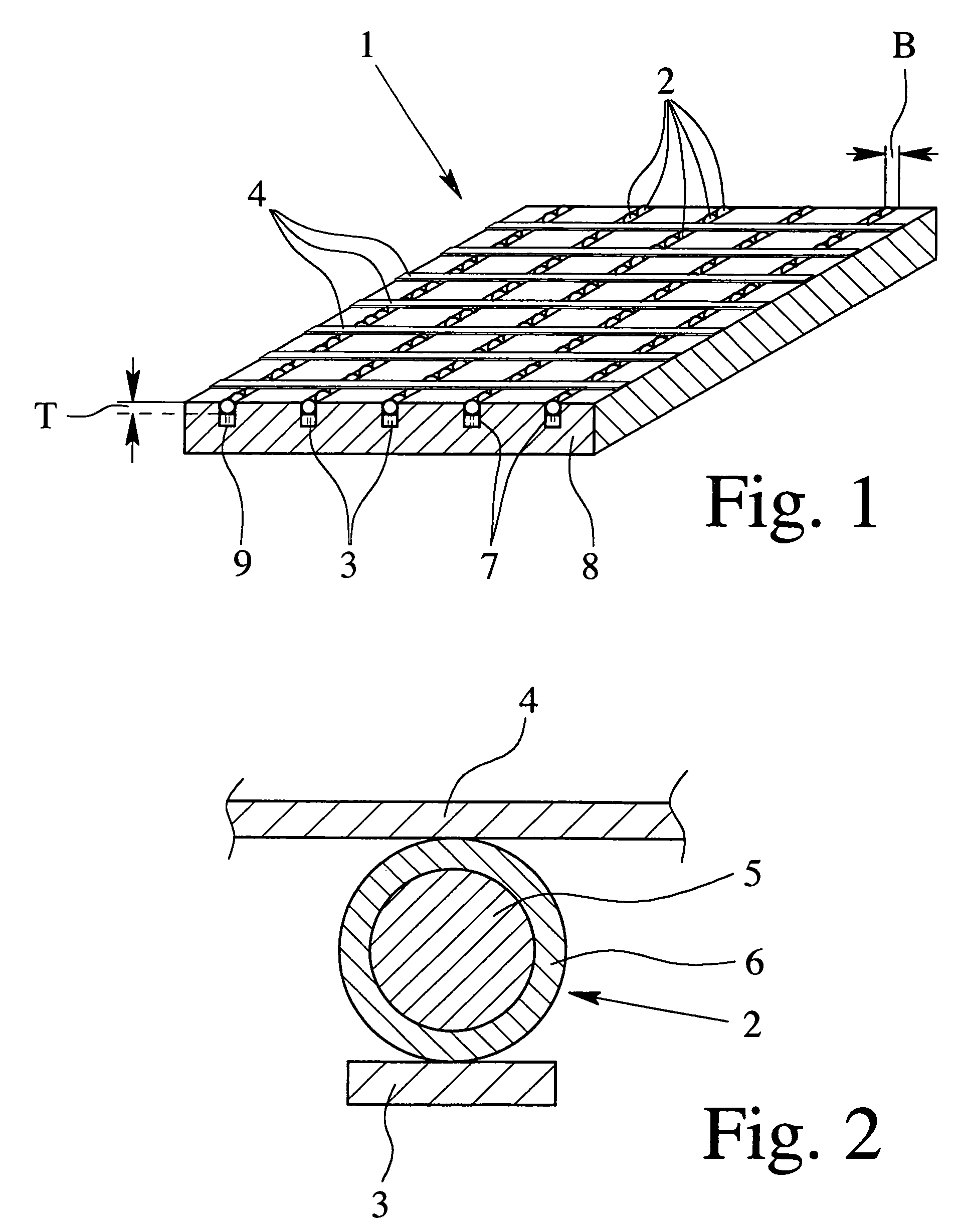
[0029]FIG. 1 shows in a schematic, perspective illustration a microelectronic component 1 according to a In particular, this embodiment concerns an electronic memory with a plurality of memory cells or transistors, preferably single-electron transistors. However, the microelectronic component 1 can also be used for other purposes.

[0030]The microelectronic component 1 has a plurality of clusters 2, which are shown in FIG. 1 in the shape of balls.

[0031]The microelectronic component 1 further has first and second connecting electrodes 3, 4 for electrical attachment or contact to clusters 2. This will be discussed in more detail below.

[0032]FIG. 2 shows in a schematic, sectional illustration the preferred design of a cluster 2. The cluster 2 has a metallic cluster nucleus 5 and a preferably electrically insulating cluster shell 6.

[0033]The cluster nucleus 5 is preferably composed of a transition metal, especially gold. Each cluster nucleus 5 comprises several metal atoms, especially at...

second embodiment

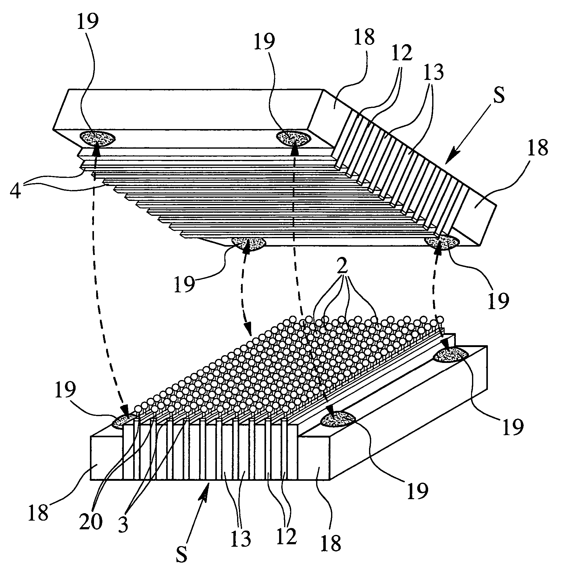
[0055]The mentioned width B for the second connecting electrodes 4 also applies preferably for the first connecting electrodes 3, especially when the clusters 2 are arranged on freely accessible first connecting electrodes 3, that is, not in the grooves 7, as explained farther below for the present invention.

[0056]As already explained in the introduction, for the shown embodiment, not all of the clusters 2 are contacted, instead only those in the region of the intersecting points between the first and second connecting electrodes 3, 4. The other, non-contacted clusters 2 are then non-critical components for the function of the microelectronic component 1, especially if there are several non-connected clusters 2 in the groove 7 between two adjacent, connected clusters 2 in a groove 7.

[0057]Naturally, as an alternative or addition, it is also possible for no other clusters 2 to be arranged between the connected clusters 2 in a groove 7 or for the chain of clusters 2 to be broken, for ...


PUM


Abstract

A micro electronic component, preferably in the form of an electronic memory, includes the use of clusters as an electronic memory. Also disclosed as part of the present invention is a method for fabricating a micro electronic component. The present invention contemplates fabrication of an especially compact electronic memory that works especially with single-electron transistors or single-electronic transfers. According to the present invention, clusters with a metallic cluster nucleus are arranged in parallel grooves essentially in lines or rows and are connected individually to first and second connecting electrodes, such that individually the clusters can be electrically modified or polled independently of each other.

Description

CROSS-REFERENCES TO RELATED APPLICATIONS[0001]The present application is a Continuation-In-Part of U.S. patent application Ser. No. 11 / 093,196, filed Mar. 29, 2005, entitled “MICRO ELECTRONIC COMPONENT” which is hereby incorporated by reference in its entirety.[0002]The present application claims the benefit of German Patent Application Serial No. 10 2004 016 534.3, filed Mar. 31, 2004; German Patent Application Serial No. 10 2004 018 915.3, filed Apr. 15, 2004; and German Patent Application Serial No. 10 2004 035 615.7, filed Jul. 22, 2004, and European Patent Application Serial No. 05016200, filed Jul. 26, 2005, all of which are hereby incorporated by reference in their entirety.BACKGROUND OF THE INVENTION[0003]The present invention relates to a microelectronic component, especially a memory, a use of clusters, and a method for fabricating a microelectronic component.[0004]From U.S. Pat. No. 5,350,930 A, a microelectronic component with at least one cluster is known. Here, micro-q...

Claims


Application Information

Patent Timeline
Patent Type & Authority Patents(United States)
IPC IPC(8): H01L23/535
CPCB82Y10/00G11C13/02H01L27/24H01L49/006H01L29/0673H01L29/155H01L29/201H01L29/7613H01L29/0665G11C2213/77Y10S977/774Y10S977/81Y10S977/94Y10S977/943H10B63/00H10N99/05
Inventor SCHMID, GUNTERSIMON, ULRICHJAGER, DIETERSANTHANAM, VENUGOPALREUTER, TORSTEN
Owner UNIV DUISBURG ESSEN
Why Eureka
Try Eureka