Shift register
a technology of shift register and drive circuit, which is applied in the direction of digital storage, counting chain synchronous pulse counters, instruments, etc., can solve the problems of malfunction of pull-down tft and tpd
- Summary
- Abstract
- Description
- Claims
- Application Information
AI Technical Summary
Benefits of technology
Problems solved by technology
Method used
Image
Examples
first embodiment
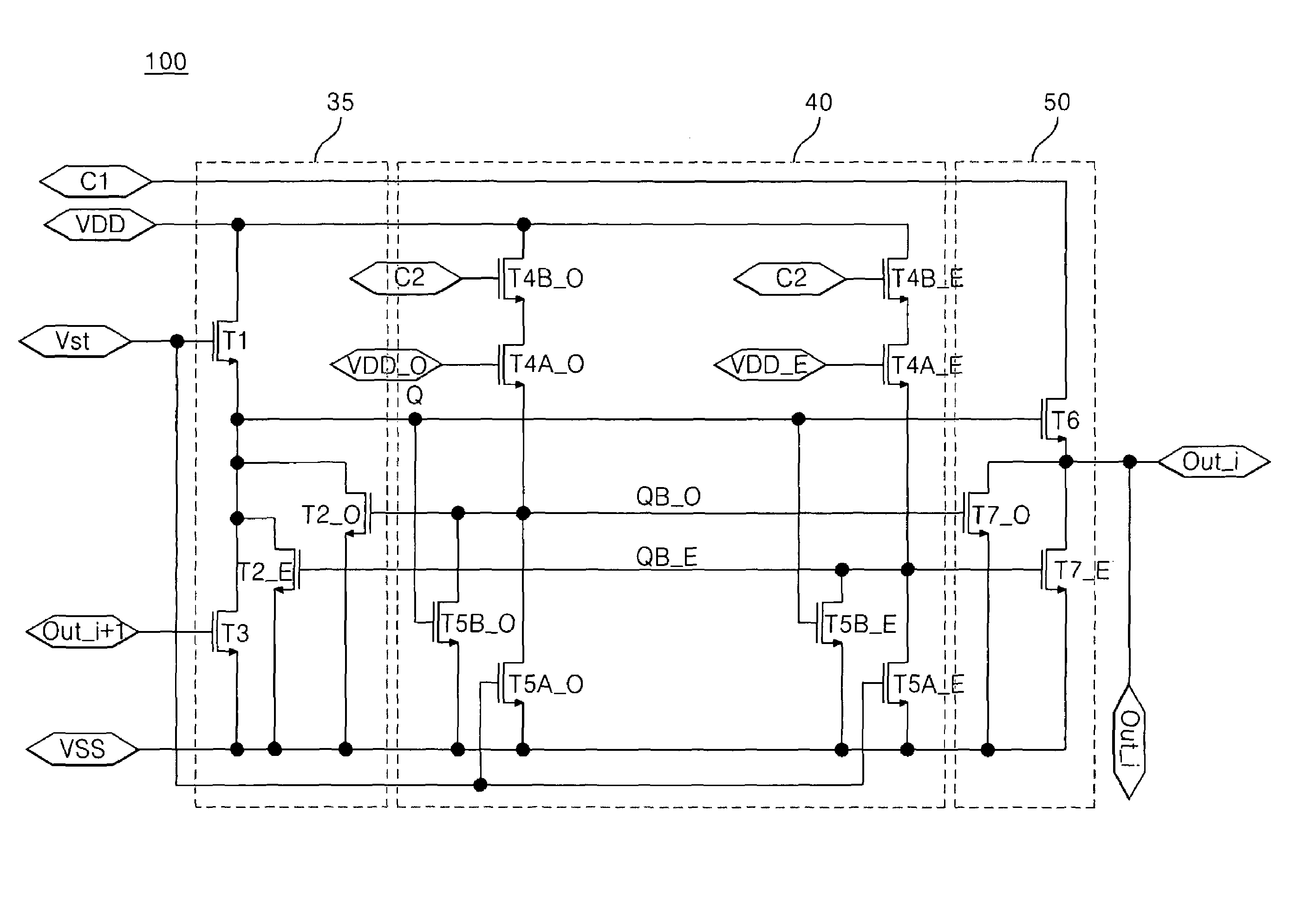
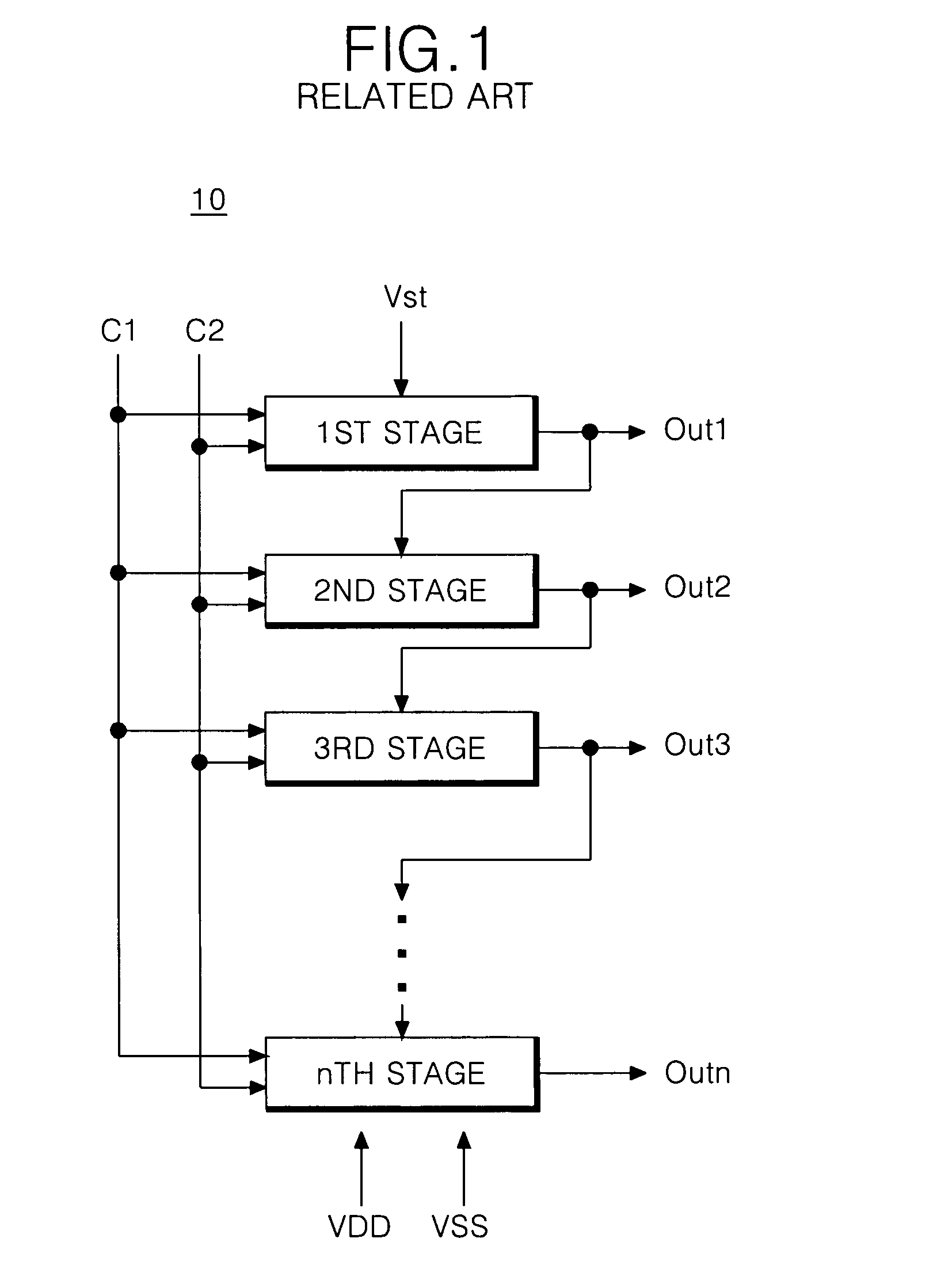
[0022]FIG. 3 illustrates a circuit diagram of one of a plurality of stages connected in cascade a shift register and FIG. 4 illustrates a driving waveform diagram for use with the stage shown in FIG. 3. The stage 100 of the shift register shown in FIG. 3 includes a first controller 35, a second controller 40 and an output buffer 50. The first controller 35 and the second controller 40 may control the output buffer 50 to output different output signals. For example, the first controller 35 and the second controller 40 may activate or deactivate thin film transistors (TFTs) of the output buffer 50. The first controller 35 and the second controller 40 may include TFTs that are activated or deactivated in response to various control signals.
[0023]The output buffer 50 includes a pull-up TFT T6 for outputting a first clock signal C1 to an output line in response to the state of a Q node. The output buffer 50 also includes odd and even pull-down TFTs T7_O, T7_E for outputting a low-level ...
second embodiment
[0040]FIG. 5 illustrates a circuit diagram of one of stages connected in cascade in a shift register according to a The stage 500 includes the same components as the stage 100 shown in FIG. 3 and further includes an even TFT T5C_E and an odd TFT T5C_O. The even TFT T5C_E discharges the QB_E node by the first AC voltage VDD_O and the odd TFT T5C_O discharges the QB_O node by the second AC voltage VDD_E.
[0041]The even TFT T5C_E, as shown in FIG. 5, is turned on to supply the low-level voltage VSS to the QB_E node if the first AC voltage VDD_O becomes the high state in the odd frame. The odd TFT T5C_O is turned on to supply the low-level voltage VSS to the QB_O node if the second AC voltage VDD_E becomes the high state in the even frame. In other words, the even TFT T5C_E changes the high-state voltage of the QB_E node to the low-state voltage by applying the low state voltage in the odd frame. The odd TFT T5C_O changes the high-state voltage of the QB_O node to the low-state voltage ...
third embodiment
[0042]FIG. 6 illustrates a circuit diagram of one of stages 600 in a shift register according to a Unlike the stage 500 of FIG. 5, the even TFT T5C_E is controlled by the QB_O node and the odd TFT T5C_O is controlled by the QB_E node in FIG. 6. Referring to FIG. 4, the even TFT T5C_E shown in FIG. 6 is turned on by the QB_O node which becomes the high state after a high output voltage Out_i is supplied in the odd frame. The QB_E node remains the low-level voltage VSS. The odd TFT T5C_O is turned on to keep the QB_O node at the low-level voltage VSS if the QB_E node become the high state in the even frame.
[0043]As described above, the shift register may drive the dual pull-down TFT T7_O, T7_E alternately in the odd frame and the even frame. As a result, the gate bias stress may be prevented. Also, the shift register drives the TFTs T4A_O, T4B_O charging the QB_O node and the TFTs T4A_E, T4B_E charging the QB_E node alternately in the odd frame and the even frame. It is possible to r...
PUM
 Abstract
Description
Claims
Application Information
 - R&D
- Intellectual Property
- Life Sciences
- Materials
- Tech Scout
- Unparalleled Data Quality
- Higher Quality Content
- 60% Fewer Hallucinations
Browse by: Latest US Patents, China's latest patents, Technical Efficacy Thesaurus, Application Domain, Technology Topic, Popular Technical Reports.
© 2025 PatSnap. All rights reserved.Legal|Privacy policy|Modern Slavery Act Transparency Statement|Sitemap|About US| Contact US: help@patsnap.com


