Luminescent device
a technology of luminescent devices and carriers, applied in the direction of discharge tube luminescnet screens, natural mineral layered products, transportation and packaging, etc., can solve the problems of further reduction of drive voltage, difficult to generate noise, and unresolved carrier moving quality of organic interfaces, etc., to improve the mobility of carriers, reduce drive voltage, and prolong service life
- Summary
- Abstract
- Description
- Claims
- Application Information
AI Technical Summary
Benefits of technology
Problems solved by technology
Method used
Image
Examples
embodiment 1
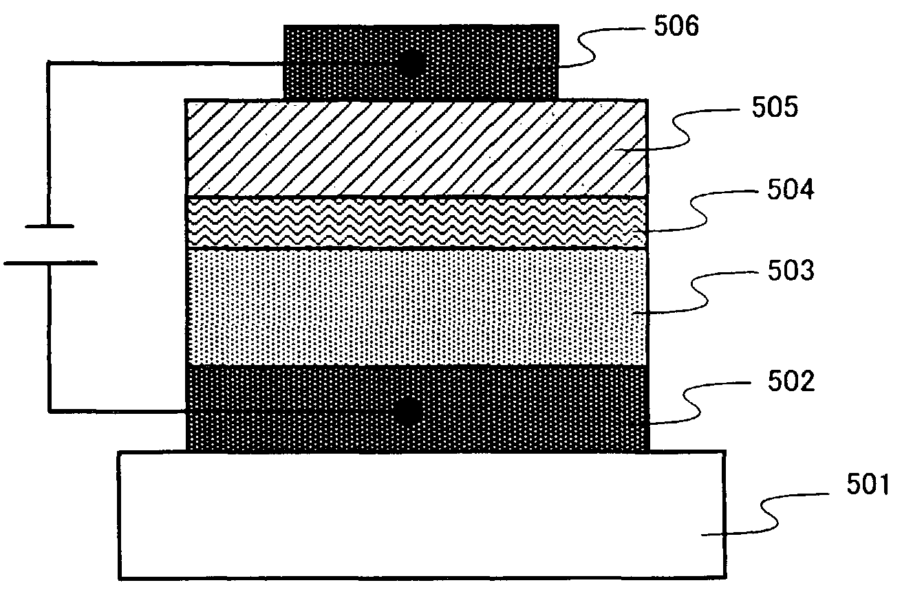
[0190]In this embodiment, there is concretely illustrated an element, to which the hole transporting mixed layer shown in FIG. 5 is applied.
[0191]First, an indium tin oxide (referred below to as “ITO”) is deposited to a film thickness of about 100 nm on a glass substrate 501 with sputtering to provide an anode 502. Subsequently, CuPc being a hole injecting material, and α-NPD being a hole transporting material, are subjected to codeposition at the deposition rate ratio 1:1 to form a hole transporting mixed layer 503, which has a film thickness of 50 nm.
[0192]Further, a layer obtained by doping rubrene of 5 wt % on Alq3 is laminated by a film thickness of 10 nm to provide a luminescent layer 504. Finally, Alq3 is deposited to a film thickness of 40 nm to provide an electron transporting layer 505, and Al:Li alloy (Li of 0.5 wt % in mass ratio) is deposited to a film thickness of about 150 nm to provide a cathode 506, so that it is possible to manufacture an organic luminescent elemen...
embodiment 2
[0193]In this embodiment, there is concretely illustrated an element, to which the electron transporting mixed layer shown in FIG. 6 is applied.
[0194]First, ITO is deposited to a film thickness of about 100 nm on a glass substrate 601 with sputtering to provide an anode 602. Subsequently, α-NPD being a hole transporting material is deposited to a film thickness of 50 nm to thereby form a hole transporting layer 603.
[0195]Further, perylene is laminated by a film thickness of 10 nm to provide a luminescent layer 604, and then BPhen being an electron transporting material, and Alq3 being an electron injecting material, are subjected to codeposition at the deposition rate ratio 1:1 to form an electron transporting mixed layer 605, which has a film thickness of 40 nm. Finally, Al:Li alloy (Li of 0.5 wt % in mass ratio) is deposited to a film thickness of about 150 nm to provide a cathode 606, so that it is possible to manufacture an organic luminescent element of blue luminescence result...
embodiment 3
[0196]In this embodiment, there is concretely illustrated an organic luminescent element obtained by inserting between an anode 2402 and an organic compound layer 2403, a hole injecting region, which is composed of a hole injecting material, in the organic luminescent element shown in FIG. 24.
[0197]First, a glass substrate 2401 is prepared, on which ITO is deposited to a film thickness of about 100 nm with sputtering to form an anode 2402. The glass substrate 2401 having the anode 2402 is carried into a vacuum chamber as shown in FIGS. 31A and 31B. In the embodiment, four kinds of materials (of which three kinds are organic compounds and one kind is a metal forming a cathode) are deposited, and so four deposition sources are necessary.
[0198]First, CuPc being a hole injecting material is deposited to a film thickness of 20 nm, and without an interval from a point of time when the film thickness of 20 nm is reached and deposition of CuPc is terminated, deposition of α-NPD being a hole...
PUM
 Abstract
Description
Claims
Application Information
 - Generate Ideas
- Intellectual Property
- Life Sciences
- Materials
- Tech Scout
- Unparalleled Data Quality
- Higher Quality Content
- 60% Fewer Hallucinations
Browse by: Latest US Patents, China's latest patents, Technical Efficacy Thesaurus, Application Domain, Technology Topic, Popular Technical Reports.
© 2025 PatSnap. All rights reserved.Legal|Privacy policy|Modern Slavery Act Transparency Statement|Sitemap|About US| Contact US: help@patsnap.com


