
Amplifier circuit with bias stage for controlling a common mode output voltage of the gain stage during device power-up

a technology of amplifier circuit and gain stage, which is applied in the direction of dc-amplifiers with dc-coupled stages, differential amplifiers, and amplifiers with semiconductor devices/discharge tubes, etc. it can solve the problems of consuming significant power, affecting the power-up sequence, so as to reduce the amount of time needed, reduce the potential difference, and reduce the power-up time

Active Publication Date: 2009-07-14
MONTEREY RES LLC
View PDF14 Cites 11 Cited by
  • Summary
  • Abstract
  • Description
  • Claims
  • Application Information

AI Technical Summary

Benefits of technology

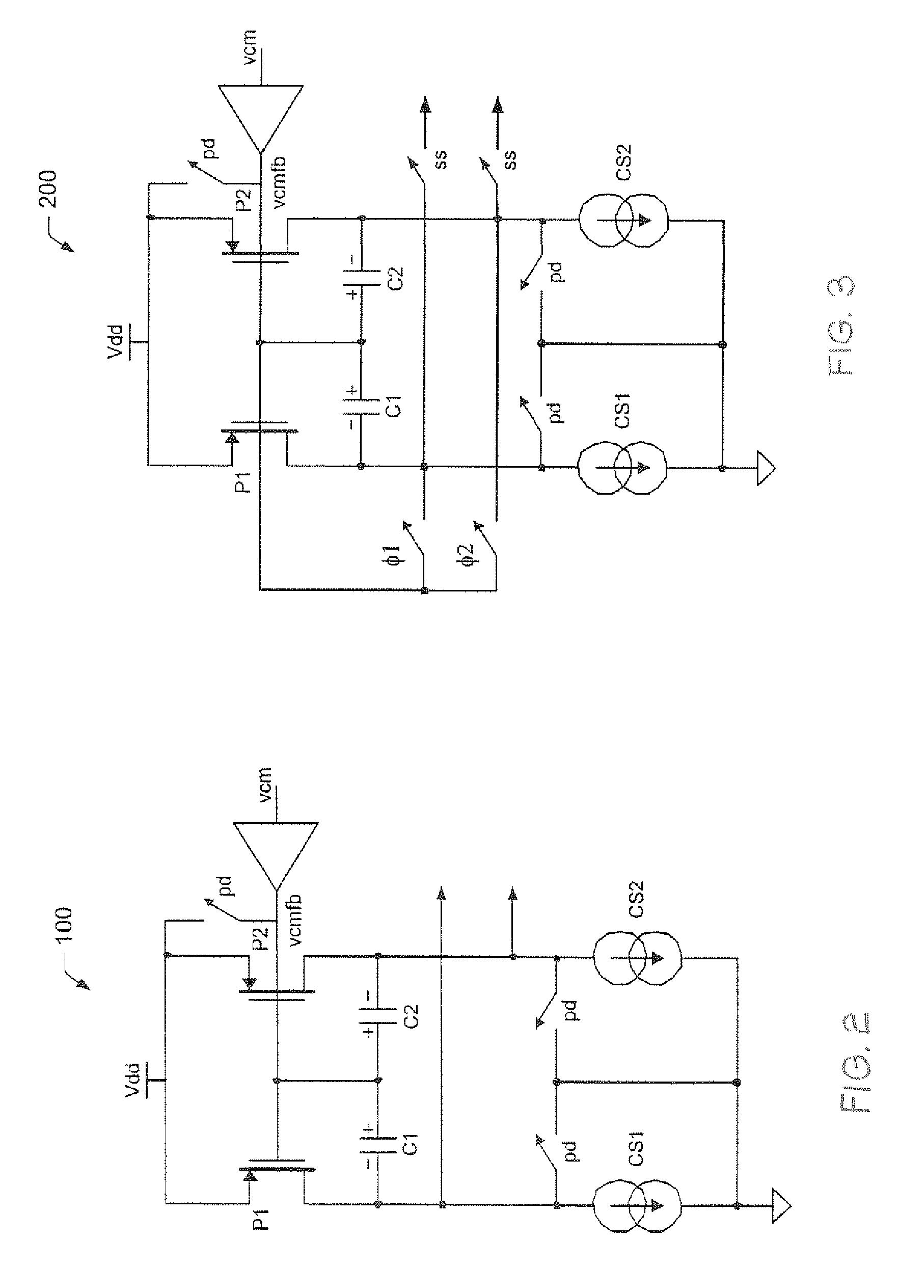
[0017]In some cases, the first voltage level may be greater than a ground potential, whereas the second voltage level may be close to the common mode feedback voltage supplied to the mutually-coupled gate terminals of the common mode feedback transistors. The bias stage may be switchably connected to the gain stage for supplying a ground referenced bias voltage to the negative terminals of the compensation capacitors and a VDD referenced bias voltage to the positive terminals of the compensation capacitors during a power-up operation. In this manner, the bias stage may reduce a potential difference between the positive and negative terminals of the compensation capacitors, thereby reducing the amount of time needed to fully charge the compensation capacitors during power-up. By controlling the manner in which both terminals are charged, the bias stage reduces the power-up time without compromising control of the voltage present at the output nodes of the gain stage.

Problems solved by technology

Unfortunately, conventional operational amplifier designs often suffer from degraded performance when supplied with a low voltage power supply.
Unfortunately, however, typical amplifier circuits that implement a power-down (or sleep state) followed by a power-up sequence before entering a normal operation condition, consume significant amounts of power or otherwise take undesirably long periods for the power-up sequence to occur.
Even so, such conventional circuits may not place the internal nodes of the gain stage at their optimal levels, taking into consideration the common mode voltage of the differential signals applied to those nodes.
However, reducing the compensation capacitor sizes can compromise amplifier stability, and increasing the current sources will increase the power consumption of the amplifier.

Method used


Image

  • Amplifier circuit with bias stage for controlling a common mode output voltage of the gain stage during device power-up
  • Amplifier circuit with bias stage for controlling a common mode output voltage of the gain stage during device power-up
  • Amplifier circuit with bias stage for controlling a common mode output voltage of the gain stage during device power-up

Examples


Embodiment Construction

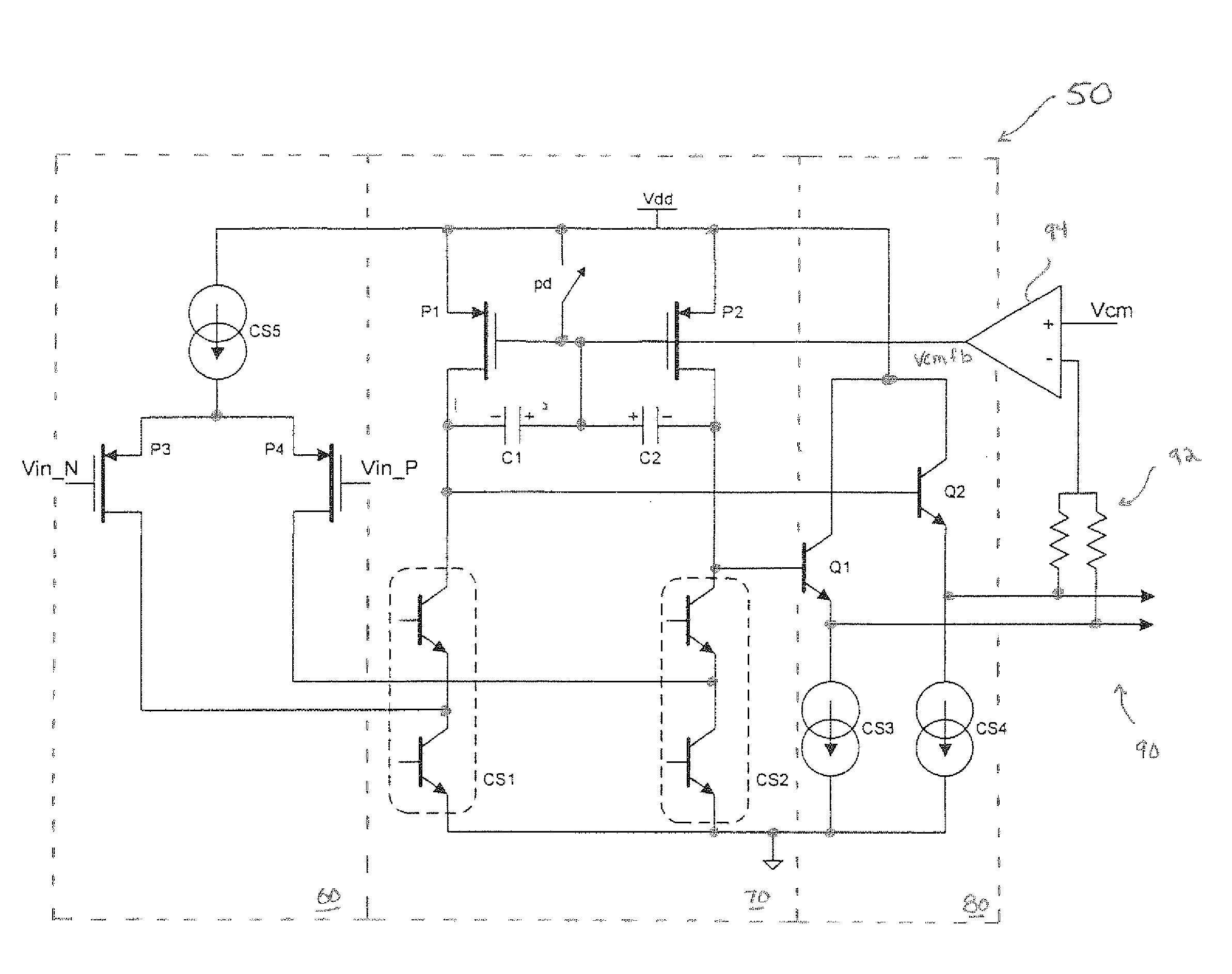
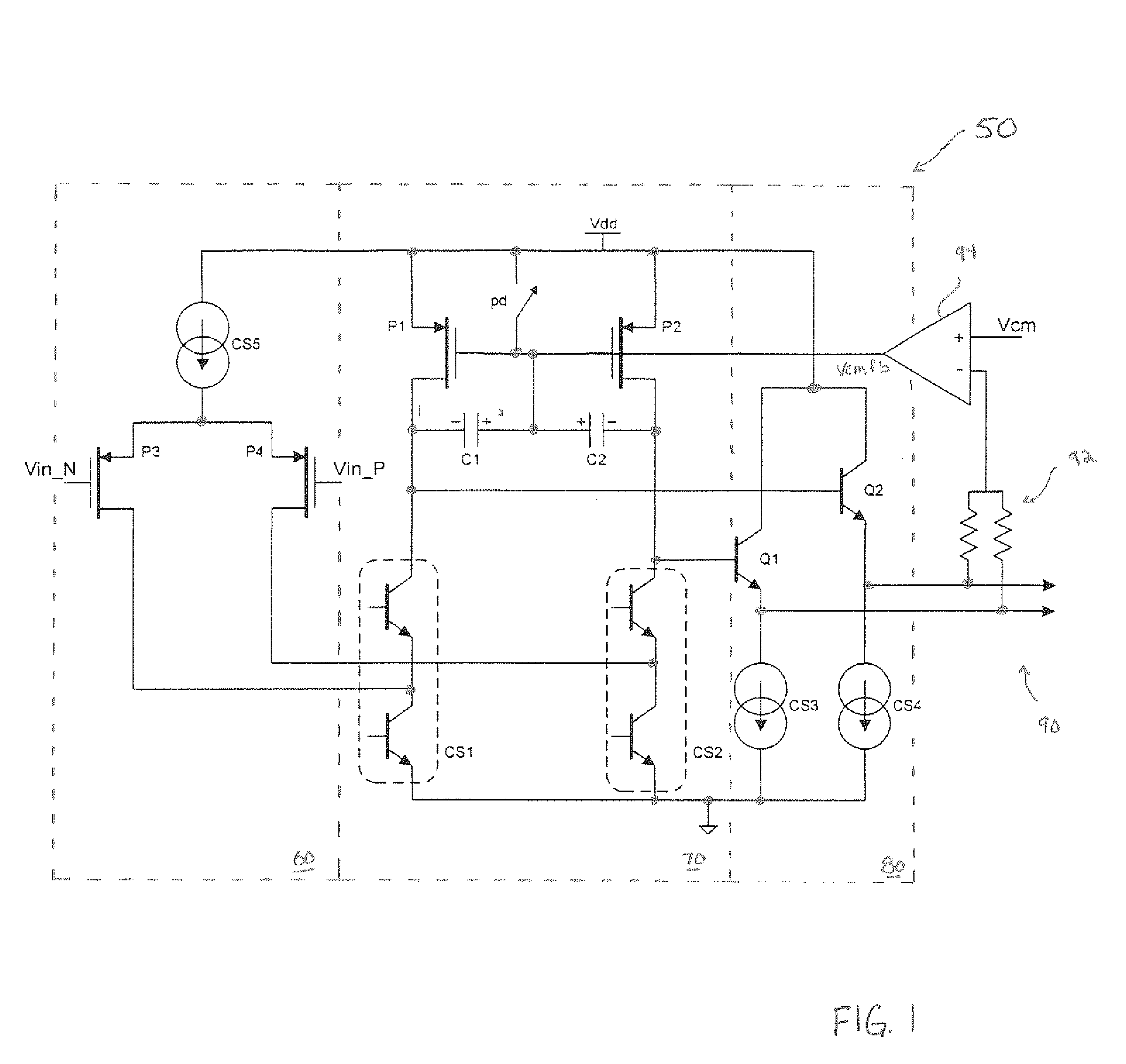
[0026]Turning now to the drawings, FIG. 1 illustrates a multi-stage amplifier 50. Amplifier 50 includes an input or Gm stage 60, a gain stage 70, an output stage 80, and a common mode feedback stage 90. Input stage 60 can receive differential inputs (Vin_N and Vin_P). Transistors P3 and P4 are coupled in cascode with a current source (CS5) to provide a gain on the output to the next stage 70. Stage 70 includes another pair of cascode-connected transistors P1 and P2, a pair of compensation capacitors (C1 and C2), and a pair of current sources (CS1 and CS2). The negative terminal of capacitors C1 and C2 are connected to the output of gain stage 70, which feeds to the input of output stage 80 and, more specifically, to the gate (or base) of transistors Q1 and Q2. Transistors Q1 and Q2 provide current at their respective emitter terminals to current sources CS3 and CS4, which produce the corresponding output from amplifier 50 and, in addition, feed a resistor-divider circuit 92 of feedb...


PUM


Abstract

An improved amplifier circuit is provided herein with a gain stage and a bias stage, which may be switchably connected to the gain stage during power-up operations. The bias stage reduces a power-up time associated with the gain stage, while minimizing current consumption in the next amplifier stage and improving battery life. For example, during power-up, the bias stage may enable the output voltage of the gain stage to gradually rise from a ground potential to a desired common mode level in a highly controlled and predictable manner. By preventing “glitches” in the output voltage, the bias stage eliminates the need for inserting switches in the signal path between the output nodes of the gain stage and input nodes of the next amplifier stage.

Description

PRIORITY CLAIM[0001]This application claims priority to U.S. Provisional Application No. 60 / 688,289 filed Jun. 7, 2005.BACKGROUND OF THE INVENTION[0002]1. Field of the Invention[0003]This invention relates to differential amplifier circuits and, more particularly, to amplifier circuit designs with reduced power-up time, reduced power consumption and improved reliability.[0004]2. Description of the Related Art[0005]The following descriptions and examples are not admitted to be prior art by virtue of their inclusion within this section.[0006]Amplifiers are often used in integrated circuit design. Even in the case of digital integrated circuits, amplifiers may be used for purposes such as providing a reference voltage for other parts of the circuit. Amplifier circuits generally include a plurality of stages, such as an input stage, a gain stage and an output stage, among others. In differential designs, a pair of differential signals may be supplied to the input stage of the amplifier,...

Claims


Application Information

Patent Timeline
Patent Type & Authority Patents(United States)
IPC IPC(8): H03F3/45
CPCH03F3/45291H03F3/45807H03F2203/45008H03F2203/45418H03F2203/45424H03F2203/45728H03F2203/45648H03F2203/45681H03F2203/45722H03F2203/45726H03F2203/45626
Inventor CETIN, JOSEPH A.SIENKO, MATTHEW D.MURIBY, JASON F.
Owner MONTEREY RES LLC
Learn More