Ion sources and methods for generating an ion beam with a controllable ion current density distribution
a technology of ion beam and density distribution, which is applied in the field of ion sources, can solve the problems of limiting the uniformity of the ibe process, the compensation method has several limitations, and the uniformity of the ion current density distribution
- Summary
- Abstract
- Description
- Claims
- Application Information
AI Technical Summary
Benefits of technology
Problems solved by technology
Method used
Image
Examples
example 1
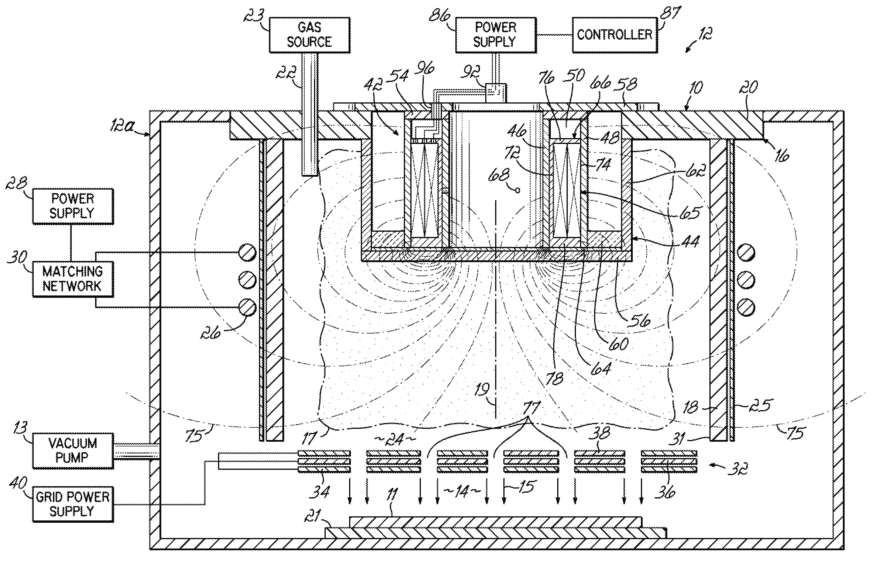
[0064]An ion source having an electromagnet assembly, otherwise substantially identical to electromagnet assembly 42b (FIG. 4) but with each of the inner and outer electromagnet coils 65, 105 including a single coil of 970 turns, was equipped with an ammeter between the coil of the radially innermost electromagnet and power supply for purposes of measuring the current supplied to the coil of this electromagnet. The coil 105 of the radially outermost electromagnet was disconnected from the power supply so that only the innermost electromagnet was energized. An electrical probe was inserted into the beam and situated in the substrate plane perpendicular to the beam incidence direction. The probe, being charged under the substrate processing, allowed measuring the voltage, which was considered as a measure of the broad ion beam neutralization.
[0065]A 1200 V, 650 mA beam of positively charged ions was extracted from an argon gas plasma. While propagating toward the substrate, the ion be...
example 2
[0069]As evidence that the operation of the electromagnet under controlled conditions does not degrade the ion beam directionality, the “local divergence angle” of the angular distribution of the ions was evaluated for optimum electromagnet current settings at different positions in the beam and compared with equivalent results obtained without the electromagnet for the same process parameters. The “local divergence angle” was determined by etching a substrate beneath a masking aperture and measuring the size of the etch spot, essentially as described by J. R. Kahn, et al, J. Vac. Sci. Technol. A14(4), July / August 1996, p. 2106-2112 (ref. FIG. 1), except that a silicon dioxide coated silicon wafer was used as the substrate and a nanospectrophometric measurement apparatus (Nanometrics Nanospec™ 8000) capable of high resolution etch depth and lateral position measurement was used to determine the etch depth profile. The disclosure of this publication is hereby incorporated by referenc...
example 3
[0072]A series of etch profiles, which have been normalized for presentation, were generated using the ion source of Example 1 and are shown in FIG. 7. With no current applied to the coils of the electromagnet, the plasma density distribution and the distribution of ion flux are characterized by a convex profile, which is reflected in the etch profile of curve 200. At a relatively low field strength, BL, the etch profile increases in convexity with increasing field strengthen, as reflected in the etch profile of curve 210. At a relatively high field strength, BH, the etch profile changes shape to become more concave with increasing field strength. Eventually, the profile itself changes to concave, as reflected in the etch profile of curve 220. At a magnetic field strength, B, between the relatively low field strength, BL, and relatively high field strength, BH, the etch profile will be essentially flat, i.e. not convex or concave, as reflected in the etch profile of curve 230. This ...
PUM
| Property | Measurement | Unit |
|---|---|---|
| pressures | aaaaa | aaaaa |
| vacuum pressure | aaaaa | aaaaa |
| frequency | aaaaa | aaaaa |
Abstract
Description
Claims
Application Information
 - R&D
- Intellectual Property
- Life Sciences
- Materials
- Tech Scout
- Unparalleled Data Quality
- Higher Quality Content
- 60% Fewer Hallucinations
Browse by: Latest US Patents, China's latest patents, Technical Efficacy Thesaurus, Application Domain, Technology Topic, Popular Technical Reports.
© 2025 PatSnap. All rights reserved.Legal|Privacy policy|Modern Slavery Act Transparency Statement|Sitemap|About US| Contact US: help@patsnap.com


