
Use of an organic matrix material for producing an organic semiconductor material, organic semiconductor material and electronic component

a technology of organic matrix material and organic semiconductor material, which is applied in the direction of discharge tube luminescnet screen, non-metal conductor, other chemical processes, etc., can solve problems such as inability to produce electronic components, and achieve the effect of high hole conductivity

Active Publication Date: 2009-06-02
NOVALED GMBH
View PDF155 Cites 55 Cited by
  • Summary
  • Abstract
  • Description
  • Claims
  • Application Information

AI Technical Summary

Benefits of technology

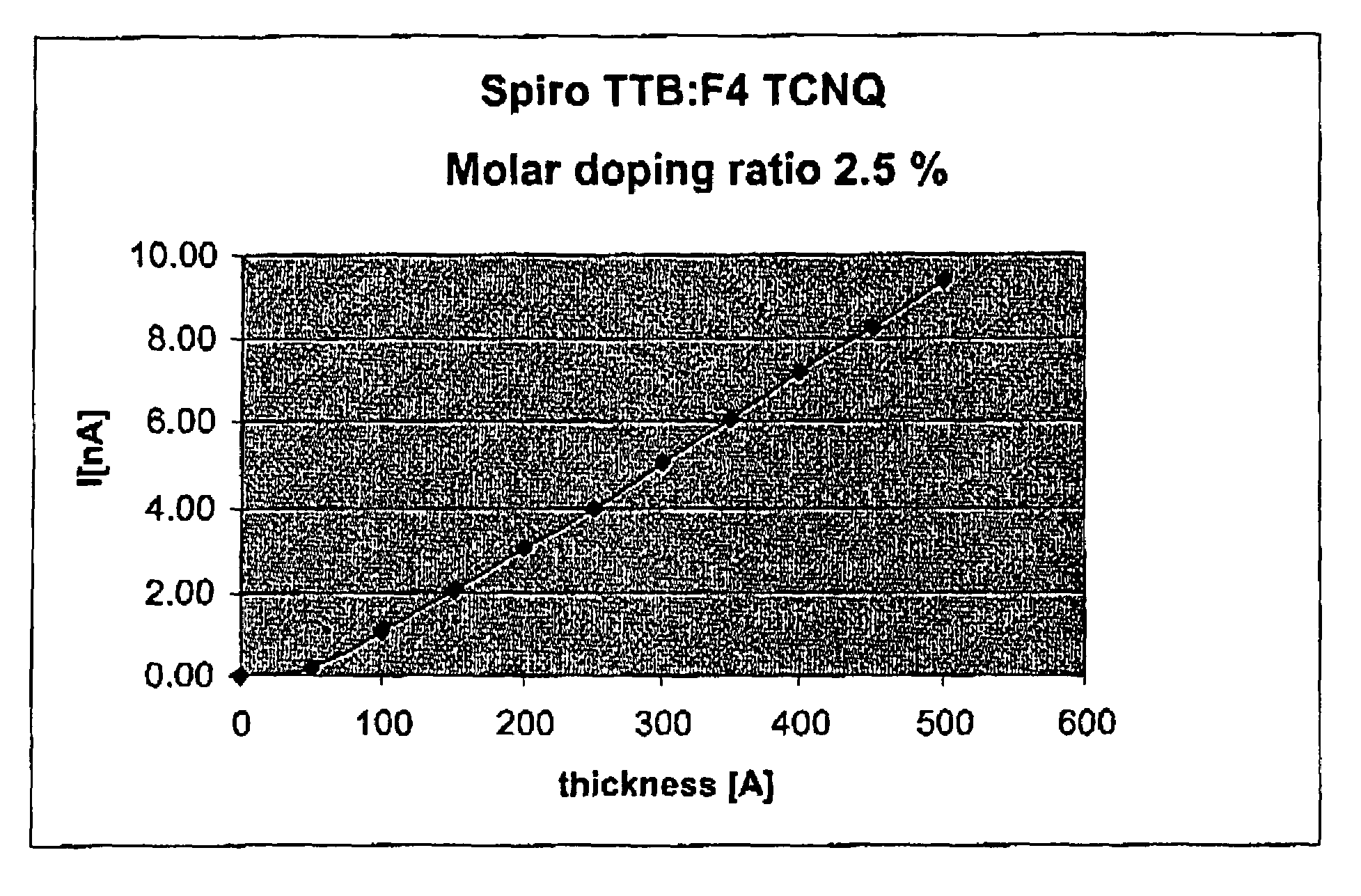
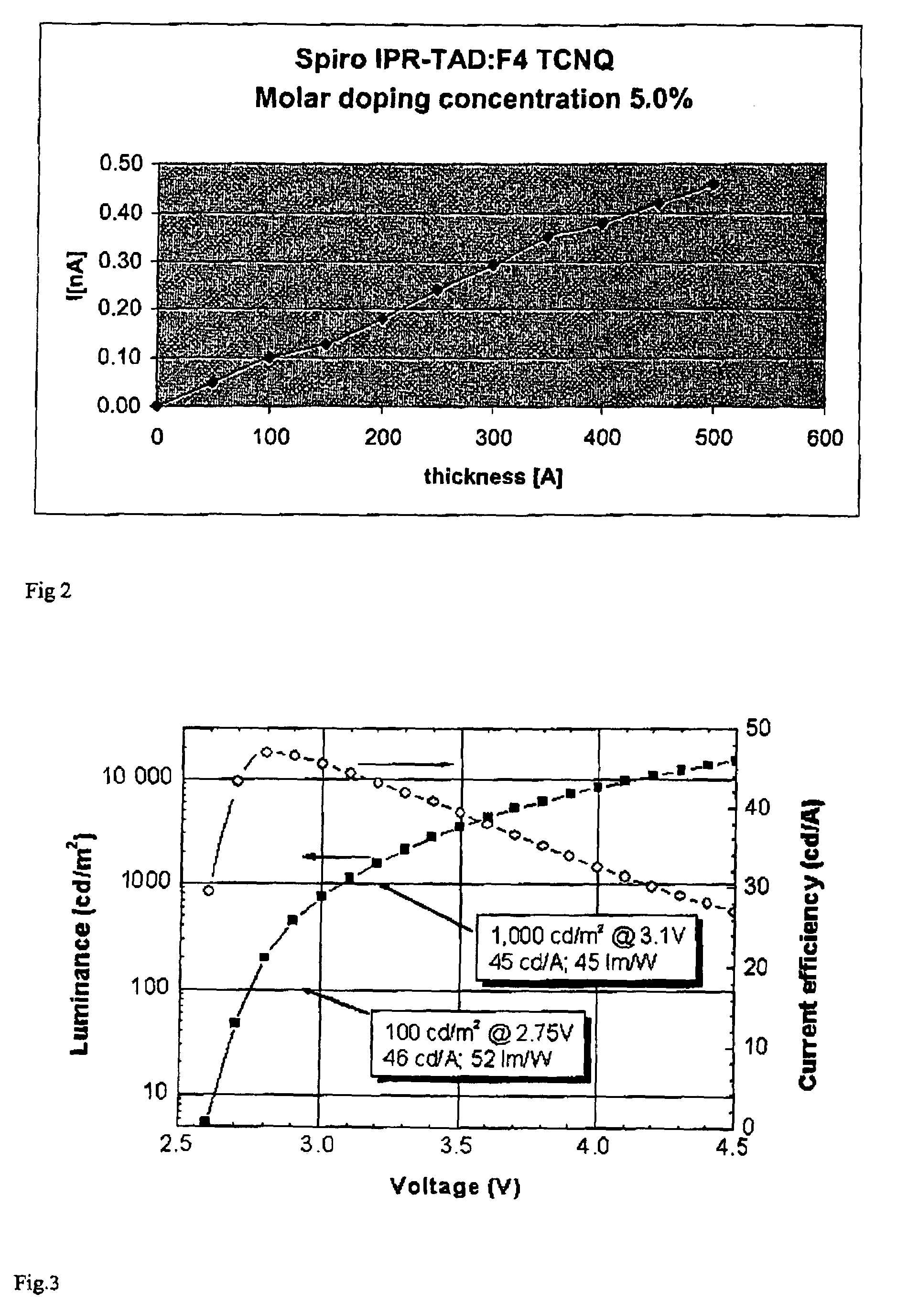
[0027]When the organic matrix materials described are used, a stable, singly positively charged cationic state of the hole transport material is achieved.

Problems solved by technology

However, these compounds are thermally unstable, i.e. they have a low glass transition temperature and tend to crystallization at low temperatures, which leads ultimately to unstable electronic components.

Method used


Image

  • Use of an organic matrix material for producing an organic semiconductor material, organic semiconductor material and electronic component
  • Use of an organic matrix material for producing an organic semiconductor material, organic semiconductor material and electronic component
  • Use of an organic matrix material for producing an organic semiconductor material, organic semiconductor material and electronic component

Examples


examples

A. Preparation of 2,2′,7,7′-tetrakis(N,N-di-p-methylphenylamino)-9,9′-spirobifluorene (spiro-TTB)

[0032]

[0033]2,2′,7,7′-Tetrabromo-9,9′-spirobifluorene (10 g, 15.8 mmol), di-p-tolylamine (14.2 g, 72.1 mmol) and sodium tert-butoxide (9.6 g, 100 mmol) are stirred in 100 ml of anhydrous toluene under nitrogen at 60° C. for 1 h. Subsequently, tri-tert-butylphosphine. (200 mg, 1.0 mmol, 6.3% based on tetrabromospirobifluorene) and palladium(II) acetate (92 mg, 0.4 mmol, 2.6% based on tetrabromospirobifluorene) are added and the reaction mixture is heated to reflux under nitrogen. The progress of the reaction is monitored by thin-layer chromatography (eluent: 50% hexane in dichloromethane). After 2.5 h, no reactant can any longer be detected in the TLC. The reaction mixture is cooled, admixed with a solution of 100 mg of KCN in 20 ml of water and stirred at 60° C. for another 1 h. After cooling to room temperature, the phases are separated, and the organic phase is dried over sodium sulpha...


PUM

PropertyMeasurementUnit
glass transition temperatureaaaaaaaaaa
temperatureaaaaaaaaaa

Abstract

The present invention relates to use of an organic matrix material for producing an organic semiconductor material, characterized in that the organic matrix material is comprised at least partly of a spirobifluorene compound, and the glass transition temperature of the organic matrix material is at least 120° C. and the highest occupied molecular orbital (HOMO) of the matrix material is at a maximum energy level of 5.4 eV; and also to an organic semiconductor material and electronic component.

Description

TECHNICAL FIELD[0001]The present invention relates to the use of an organic matrix material for producing an organic semiconductor material, and also to an organic semiconductor material comprising an organic matrix material and an organic dopant, and also to an electronic component.BACKGROUND OF THE INVENTION[0002]It is known that doping can alter organic semiconductors with regard to their electrical properties, in particular their electrical conductivity, as is also the case for inorganic semiconductors such as silicon semiconductors.[0003]In this case, generation of charge carriers in a matrix material increases the initially quite low conductivity and, depending on the type of the dopant used, achieves a change in the Fermi level of the semiconductor. Doping leads to an increase in the conductivity of the charge transport layer, which reduces resistance losses, and leads to an improved transition of the charge carriers between contacts and organic layer.[0004]For the doping of ...

Claims


Application Information

Patent Timeline
Patent Type & Authority Patents(United States)
IPC IPC(8): H01B1/00H01J1/62H01L29/08H01L31/00
CPCC09K11/06H01L51/006H05B33/14C09K2211/1007C09K2211/1011C09K2211/1014H01L51/5048Y02E10/549H10K85/633H10K50/14C09K3/00
Inventor PFEIFFER, MARTINBLOCHWITZ-NIMOTH, JANLUX, ANDREASALBECK, JOSEF
Owner NOVALED GMBH
Learn More