Pattern recognition matching for bright field imaging of low contrast semiconductor devices

a semiconductor device and bright field technology, applied in the field of bright field pattern recognition of low contrast semiconductor devices, can solve the problems of low contrast wafers, prior art pattern recognition methods are not robust enough to handle trivial deviation of low contrast images between systems, and the pattern recognition image generally shows a low pattern contrast. achieve the effect of facilitating the matching of one system, facilitating pattern recognition matching, and increasing the rate of recognition success

Inactive Publication Date: 2009-05-26
KLA TENCOR TECH CORP
View PDF11 Cites 4 Cited by
  • Summary
  • Abstract
  • Description
  • Claims
  • Application Information

AI Technical Summary

Benefits of technology

[0009]Such calibration of bright field systems greatly reduces pattern recognition failure and allows for repeatable pattern recognition of the same feature on different bright field systems.

Problems solved by technology

Unfortunately, when a wafer has a thicker and more opaque film, the pattern recognition images generally show a low pattern contrast.
Such, low contrast wafers present a challenge for prior art pattern recognition techniques.
Prior art methods of pattern recognition are not robust enough to handle trivial deviation of low contrast images between systems.
These trivial variations can lead to failure of pattern recognition matching.

Method used


Image

  • Pattern recognition matching for bright field imaging of low contrast semiconductor devices
  • Pattern recognition matching for bright field imaging of low contrast semiconductor devices
  • Pattern recognition matching for bright field imaging of low contrast semiconductor devices

Examples


Embodiment Construction

[0017]Although the following detailed description contains many specific details for the purposes of illustration, anyone of ordinary skill in the art will appreciate that many variations and alterations to the following details are within the scope of the invention. Accordingly, the embodiments of the invention described below are set forth without any loss of generality to, and without imposing limitations upon, the claimed invention.

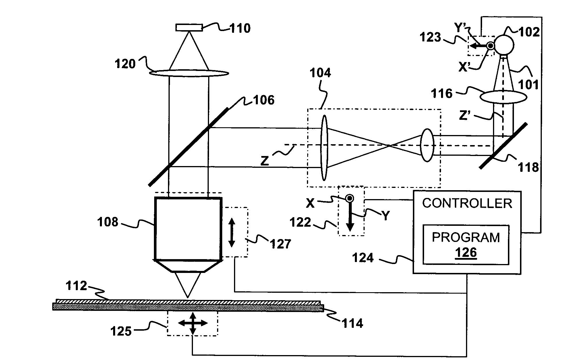
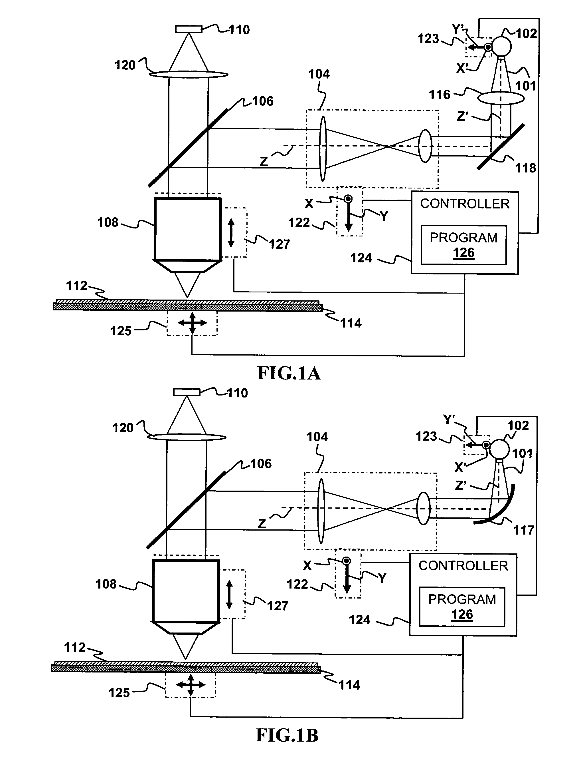
[0018]Embodiments of the present invention allow for transportability of pattern recognition recipes between bright field systems for low contrast substrates. FIGS. 1A-1B depict examples of bright field imaging systems according to embodiments of the present invention. In embodiments of the present invention, bright field imaging systems are modified to be calibrated for imaging low contrast substrates with a high rate of success of image pattern matching. In general a bright field imaging system 100 includes a light source 102, beam shaping and relay...


PUM


Abstract

Calibration of pattern recognition in bright field imaging systems is disclosed. A target pattern on a substrate on the stage is brought into focus of a bright field system. The image is scanned in a first direction while measuring an edge scattering pattern from a feature of the target pattern. The edge scattering pattern is characterized by first and second peaks. A position of the bright field system's illuminator or beam shaping and relay optics is adjusted perpendicular to an optical path until the first and second peaks are approximately equal in height.

Description

FIELD OF THE INVENTION[0001]This invention generally relates to pattern recognition for bright field imaging systems and methods. More particularly, this invention relates to bright field pattern recognition of low contrast semiconductor devices.BACKGROUND OF THE INVENTION[0002]In a conventional method for recognizing patterns, the object patterns are compared and collated with template patterns previously registered, and a decision is made that the template pattern having the least degree of mismatching (or most degree of matching) is identified as the object pattern. In semiconductor wafer processing, pattern recognition is used, e.g., for wafer alignment. A pattern recognition method typically involves memorizing the pattern of a specified characteristic area, i.e. the key pattern, on the surface of a semiconductor wafer located at a predetermined position, and the position of the key pattern, and detecting the same pattern as the key pattern at other locations on the surface of ...

Claims


Application Information

Patent Timeline
Patent Type & Authority Patents(United States)
IPC IPC(8): G01J1/10
CPCG03F9/7011G03F9/7019G03F9/7069G03F9/7088
Inventor SHEN, WEI-NINGTIAN, XINKANGHWANG, BYEONG SUTRAN, TUAN VAN
Owner KLA TENCOR TECH CORP
Why Eureka
Try Eureka