Light emitting device
a technology of light emitting devices and light sources, which is applied in the direction of resistor details, overvoltage protection resistors, and emergency protective arrangements for limiting excess voltage/current, etc., can solve the problem of more difficult to diffuse the heat generated by semiconductor light emitting elements, and achieves reduced mounting area, reduced mounting costs, and easy mounting
- Summary
- Abstract
- Description
- Claims
- Application Information
AI Technical Summary
Benefits of technology
Problems solved by technology
Method used
Image
Examples
first embodiment
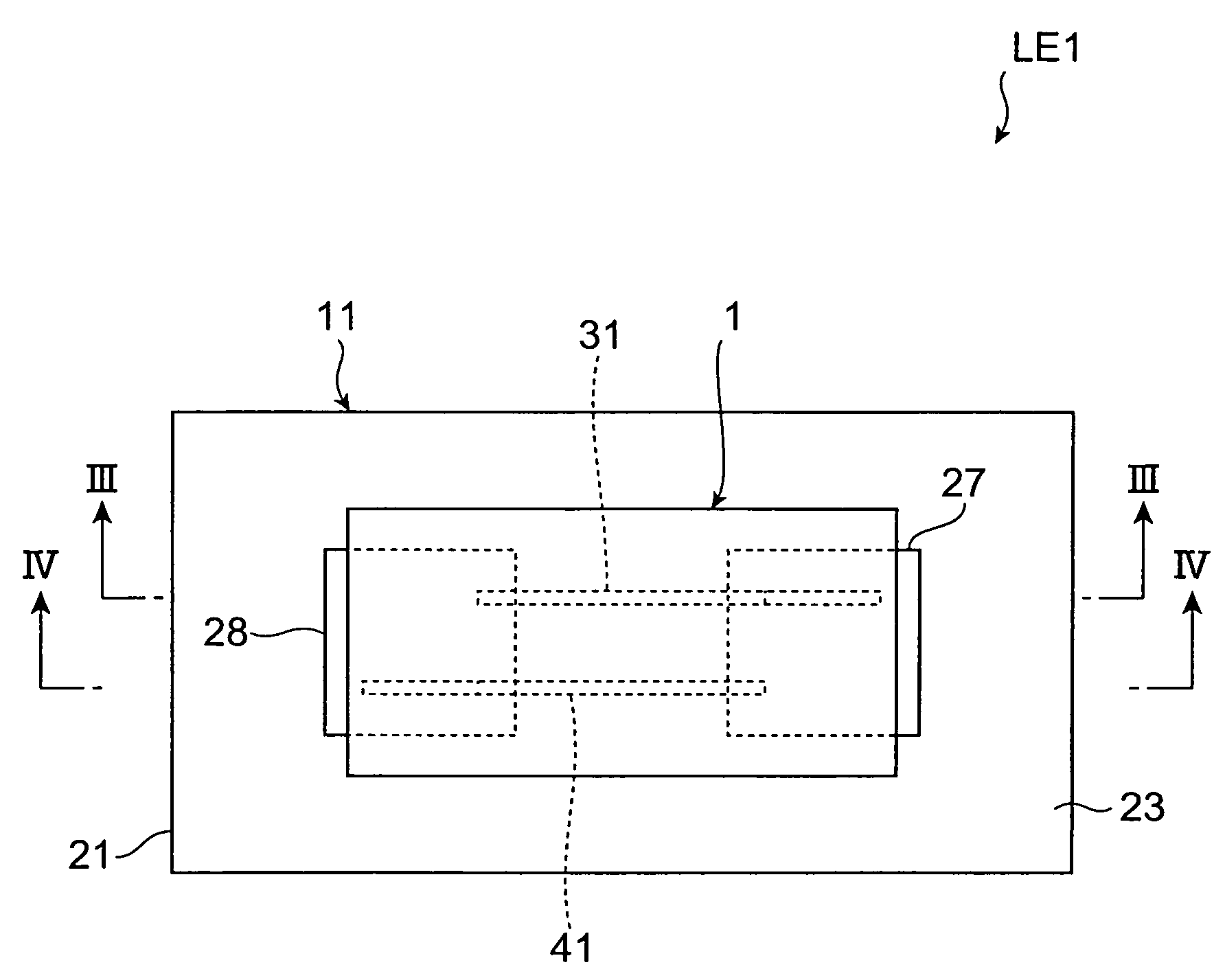
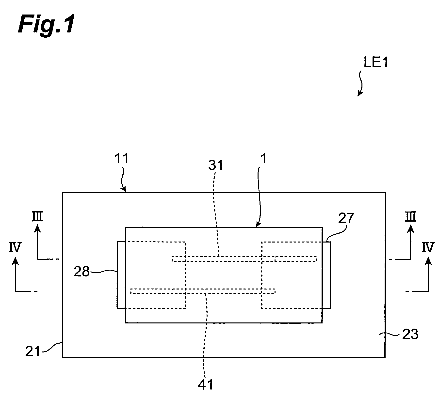
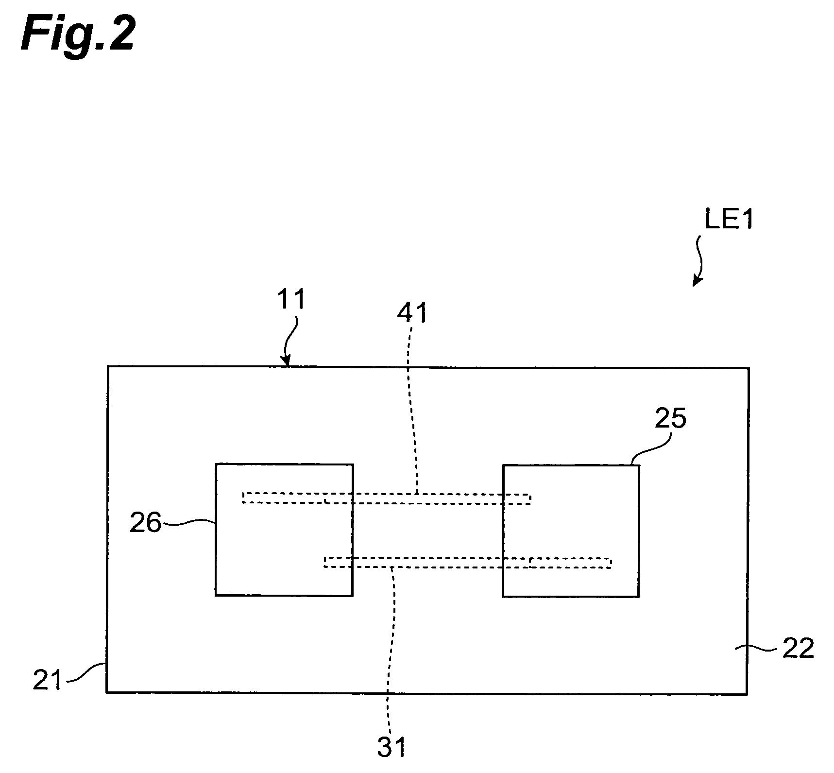
[0064]A configuration of light emitting device LE1 according to the first embodiment will be described with reference to FIGS. 1 to 4. FIG. 1 is a schematic top view showing the light emitting device of the first embodiment. FIG. 2 is a schematic bottom view showing the light emitting device of the first embodiment. FIG. 3 is a view for explaining a sectional configuration along line III-III in FIG. 1. FIG. 4 is a view for explaining a sectional configuration along line IV-IV in FIG. 1.
[0065]The light emitting device LE1, as shown in FIGS. 1 to 4, comprises a semiconductor light emitting element 1 and a multilayer chip varistor 11. The semiconductor light emitting element 1 is disposed on the multilayer chip varistor 11.
[0066]First, a configuration of multilayer chip varistor 11 will be described. The multilayer chip varistor 11 comprises a varistor element body 21 of an approximately rectangular parallelepiped shape, a plurality of (a pair of, in the present embodiment) first exter...
second embodiment
[0108]A configuration of light emitting device LE2 according to the second embodiment will be described with reference to FIG. 7. FIG. 7 is a view for explaining a sectional configuration of the light emitting device according to the second embodiment. The light emitting device LE2 of the second embodiment is different in the configuration of the multilayer chip varistor from the light emitting device LE1 of the first embodiment.
[0109]The light emitting device LE2, as shown in FIG. 7, comprises a semiconductor light emitting element 1 and a multilayer chip varistor 51. The semiconductor light emitting element 1 is disposed on the multilayer chip varistor 51. The multilayer chip varistor 51 comprises 5 a multilayer body 53, and a pair of external electrodes 55, 56. The pair of external electrodes 55, 56 are disposed each on outer surfaces of multilayer body 53. The external electrode 55 functions as an input terminal electrode of the multilayer chip varistor 51, and the external elec...
third embodiment
[0123]A configuration of light emitting device LE3 according to the third embodiment will be described with reference to FIGS. 8 and 9. FIG. 8 is a view for explaining a sectional configuration of the light emitting device according to the third embodiment. FIG. 9 is a view for explaining a sectional configuration along line IX-IX in FIG. 8. The light emitting device LE3 of the third embodiment is different in the configuration of the multilayer chip varistor from the light emitting device LE1 of the first embodiment.
[0124]The light emitting device LE3, as shown in FIGS. 8 and 9, comprises a semiconductor light emitting element 1 and a multilayer chip varistor 71. The semiconductor light emitting element 1 is disposed on the multilayer chip varistor 71.
[0125]The multilayer chip varistor 71 comprises a multilayer body 53, and a pair of external electrodes 55, 56 as the multilayer chip varistor 51 of the second embodiment does. In the multilayer chip varistor 71, a plurality of intern...
PUM
 Abstract
Description
Claims
Application Information
 - R&D
- Intellectual Property
- Life Sciences
- Materials
- Tech Scout
- Unparalleled Data Quality
- Higher Quality Content
- 60% Fewer Hallucinations
Browse by: Latest US Patents, China's latest patents, Technical Efficacy Thesaurus, Application Domain, Technology Topic, Popular Technical Reports.
© 2025 PatSnap. All rights reserved.Legal|Privacy policy|Modern Slavery Act Transparency Statement|Sitemap|About US| Contact US: help@patsnap.com


